|
|
|
PDF 24C01C Data sheet ( Hoja de datos )
| Número de pieza | 24C01C | |
| Descripción | 1K 5.0V I2C Serial EEPROM | |
| Fabricantes | MicrochipTechnology | |
| Logotipo | ||
Hay una vista previa y un enlace de descarga de 24C01C (archivo pdf) en la parte inferior de esta página. Total 30 Páginas | ||
|
No Preview Available !
24C01C
1K 5.0V I2C™ Serial EEPROM
Features:
• Single Supply with Operation from 4.5V to 5.5V
• Low-Power CMOS Technology:
- Read current 1 mA, max.
- Standby current 5 A, max.
• 2-Wire Serial Interface, I2C™ Compatible
• Cascadable up to Eight Devices
• Schmitt Trigger Inputs for Noise Suppression
• Output Slope Control to Eliminate Ground Bounce
• 100 kHz and 400 kHz Clock Compatibility
• Page Write Time 1 ms max.
• Self-Timed Erase/Write Cycle
• 16-Byte Page Write Buffer
• ESD Protection >4000V
• More than 1 Million Erase/Write Cycles
• Data Retention >200 Years
• Factory Programming Available
• Packages include 8-lead PDIP, SOIC, TSSOP,
DFN, TDFN, MSOP and 6-lead SOT-23
• Pb-Free and RoHS Compliant
• Temperature Ranges:
- Industrial (I):
- Automotive (E):
-40C to +85C
-40C to +125C
Description:
The Microchip Technology Inc. 24C01C is a 1K bit
Serial Electrically Erasable PROM with a voltage range
of 4.5V to 5.5V. The device is organized as a single
block of 128 x 8-bit memory with a 2-wire serial
interface. Low-current design permits operation with
max. standby and active currents of only 5 A and 1
mA, respectively. The device has a page write capabil-
ity for up to 16 bytes of data and has fast write cycle
times of only 1 ms for both byte and page writes. Func-
tional address lines allow the connection of up to eight
24C01C devices on the same bus for up to 8K bits of
contiguous EEPROM memory. The device is available
in the standard 8-pin PDIP, 8-pin SOIC (3.90 mm),
8-pin 2x3 DFN and TDFN, 8-pin MSOP and TSSOP
packages. The 24C01C is also available in the 6-lead
SOT-23 package.
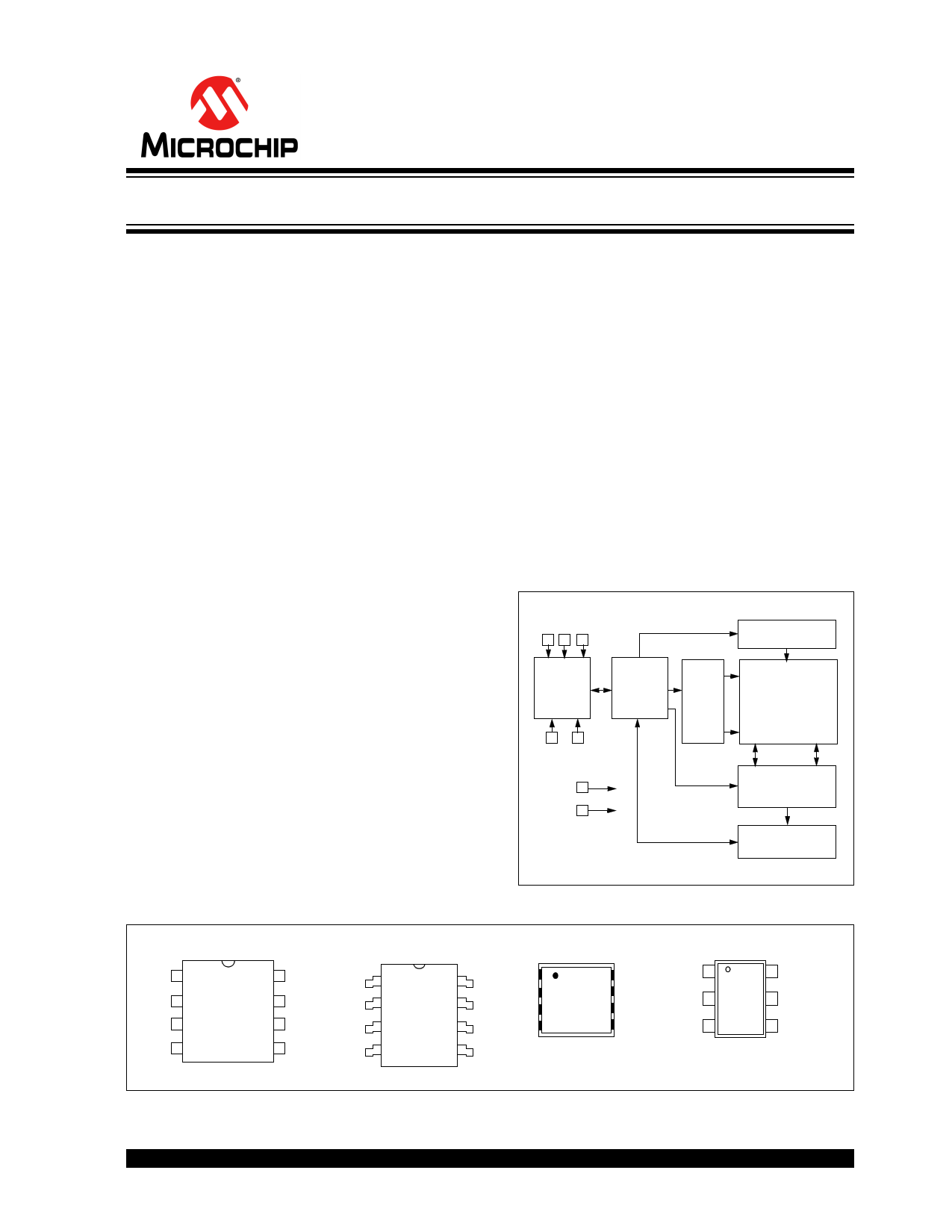
Block Diagram
A0 A1 A2
HV Generator
I/O
Control
Logic
Memory
Control
Logic
XDEC
EEPROM
Array
SDA SCL
VCC
VSS
YDEC
Sense Amp.
R/W Control
Package Types
PDIP, MSOP
A0 1
A1 2
A2 3
VSS 4
8 VCC
7 Test
6 SCL
5 SDA
SOIC, TSSOP
DFN/ TDFN
A0 1
A1 2
A2 3
VSS 4
8 VCC
7 Test
A0 1
A1 2
A2 3
6 SCL VSS 4
5 SDA
8 VCC
7 Test
6 SCL
5 SDA
SCL
VSS
SDA
SOT-23
16
25
34
VCC
A0
A1
1997-2012 Microchip Technology Inc.
DS21201K-page 1
1 page 
24C01C
2.0 PIN DESCRIPTIONS
The descriptions of the pins are listed in Table 2-1.
TABLE 2-1: PIN FUNCTION TABLE
Name
8-pin
PDIP
8-pin
SOIC
8-pin
TSSOP
A0
A1
A2
VSS
SDA
SCL
Test
VCC
111
222
333
444
555
666
777
888
8-pin
MSOP
1
2
3
4
5
6
7
8
8-pin
DFN/TDFN
1
2
3
4
5
6
7
8
SOT-23
Function
5 Chip Select
4 Chip Select
— Chip Select
2 Ground
3 Serial Data
1 Serial Clock
— Test
6 +4.5V to 5.5V Power Supply
2.1 SDA Serial Data
This is a bidirectional pin used to transfer addresses
and data into and data out of the device. It is an open
drain terminal; therefore, the SDA bus requires a pull-
up resistor to VCC (typical 10 k for 100 kHz, 2 k for
400 kHz).
For normal data transfer SDA is allowed to change only
during SCL low. Changes during SCL high are
reserved for indicating the Start and Stop conditions.
2.5 Noise Protection
The 24C01C employs a VCC threshold detector circuit
which disables the internal erase/write logic if the VCC
is below 3.8 volts at nominal conditions.
The SCL and SDA inputs have Schmitt Trigger and
filter circuits which suppress noise spikes to assure
proper device operation even on a noisy bus.
2.2 SCL Serial Clock
This input is used to synchronize the data transfer from
and to the device.
2.3 A0, A1, A2
The levels on these inputs are compared with the
corresponding bits in the slave address. The chip is
selected if the compare is true.
Up to eight 24C01C devices may be connected to the
same bus by using different Chip Select bit combina-
tions. These inputs must be connected to either VCC or
VSS.
For the SOT-23 devices up to four devices may be con-
nected to the same bus using different Chip Select bit
combinations.
In most applications, the chip address inputs A0, A1
and A2 are hard-wired to logic ‘0’ or logic ‘1’. For
applications in which these pins are controlled by a
microcontroller or other programmable device, the chip
address pins must be driven to logic ‘0’ or logic ‘1’
before normal device operation can proceed.
2.4 Test
This pin is utilized for testing purposes only. It may be
tied high, tied low or left floating.
1997-2012 Microchip Technology Inc.
DS21201K-page 5
5 Page 
24C01C
8.0 READ OPERATION
Read operations are initiated in the same way as write
operations with the exception that the R/W bit of the
slave address is set to one. There are three basic types
of read operations: current address read, random read
and sequential read.
8.1 Current Address Read
The 24C01C contains an address counter that main-
tains the address of the last word accessed, internally
incremented by one. Therefore, if the previous read
access was to address n, the next current address read
operation would access data from address n + 1. Upon
receipt of the slave address with the R/W bit set to one,
the 24C01C issues an acknowledge and transmits the
eight-bit data word. The master will not acknowledge
the transfer, but does generate a Stop condition and the
24C01C discontinues transmission (Figure 8-1).
FIGURE 8-1:
Bus Activity
Master
SDA Line
Bus Activity
S
T
A
R
T
S
CURRENT ADDRESS
READ
Control
Byte
A
C
K
Data
S
T
O
P
P
N
O
A
C
K
8.2 Random Read
Random read operations allow the master to access
any memory location in a random manner. To perform
this type of read operation, first the word address must
be set. This is done by sending the word address to the
24C01C as part of a write operation.
After the word address is sent, the master generates a
Start condition following the acknowledge. This
terminates the write operation, but not before the
internal Address Pointer is set. Then the master issues
the control byte again but with the R/W bit set to a one.
The 24C01C will then issue an acknowledge and trans-
mits the eight bit data word. The master will not
acknowledge the transfer, but does generate a Stop
condition and the 24C01C discontinues transmission
(Figure 8-2). After this command, the internal address
counter will point to the address location following the
one that was just read.
8.3 Sequential Read
Sequential reads are initiated in the same way as a
random read except that after the 24C01C transmits
the first data byte, the master issues an acknowledge
as opposed to a Stop condition in a random read. This
directs the 24C01C to transmit the next sequentially
addressed 8-bit word (Figure 8-3).
To provide sequential reads the 24C01C contains an
internal Address Pointer which is incremented by one
at the completion of each operation. This Address
Pointer allows the entire memory contents to be serially
read during one operation. The internal Address
Pointer will automatically roll over from address 7F to
address 00.
FIGURE 8-2:
RANDOM READ
Bus Activity
Master
S
T
A
R
T
Control
Byte
SDA Line
S
Bus Activity
Word
Address (n)
A
C
K
S
T
A
R
T
S
A
C
K
FIGURE 8-3:
SEQUENTIAL READ
Control
Byte
Data (n)
S
T
O
P
P
AN
CO
K
A
C
K
Bus Activity
Master
Control
Byte
Data n
Data n + 1
Data n + 2
Data n + X
SDA Line
Bus Activity
A
C
K
A
C
K
AA
CC
KK
S
T
O
P
P
N
O
A
C
K
1997-2012 Microchip Technology Inc.
DS21201K-page 11
11 Page | ||
| Páginas | Total 30 Páginas | |
| PDF Descargar | [ Datasheet 24C01C.PDF ] | |
Hoja de datos destacado
| Número de pieza | Descripción | Fabricantes |
| 24C01 | 1K/2K/4K 5.0V I2C Serial EEPROMs | MicrochipTechnology |
| 24C01 | 2-WireSerialEEPROM | ATMELCorporation |
| 24C01 | (24C01 - 24C16) 2-WIRE SERIAL CMOS EEPROM | ISSI |
| 24C01 | 1K/2K ELECTRICALLY ERASABLE PROGRAMMABLE ROM | Turbo IC |
| Número de pieza | Descripción | Fabricantes |
| SLA6805M | High Voltage 3 phase Motor Driver IC. |
Sanken |
| SDC1742 | 12- and 14-Bit Hybrid Synchro / Resolver-to-Digital Converters. |
Analog Devices |
|
DataSheet.es es una pagina web que funciona como un repositorio de manuales o hoja de datos de muchos de los productos más populares, |
| DataSheet.es | 2020 | Privacy Policy | Contacto | Buscar |