|
|
|
PDF 240VA Data sheet ( Hoja de datos )
| Número de pieza | 240VA | |
| Descripción | In-SystemProgrammable3.3VGenericDigitalCrosspointTM | |
| Fabricantes | LatticeSemiconductor | |
| Logotipo | ||
Hay una vista previa y un enlace de descarga de 240VA (archivo pdf) en la parte inferior de esta página. Total 25 Páginas | ||
|
No Preview Available !
ispGDXTM240VA
In-System Programmable
3.3V Generic Digital CrosspointTM
Features
Functional Block Diagram
• IN-SYSTEM PROGRAMMABLE GENERIC DIGITAL
CROSSPOINT FAMILY
— Advanced Architecture Addresses Programmable
PCB Interconnect, Bus Interface Integration and
Jumper/Switch Replacement
— “Any Input to Any Output” Routing
— Fixed HIGH or LOW Output Option for Jumper/DIP
Switch Emulation
— Space-Saving PQFP and BGA Packaging
— Dedicated IEEE 1149.1-Compliant Boundary Scan
Test
• HIGH PERFORMANCE E2CMOS® TECHNOLOGY
— 3.3V Core Power Supply
— 4.5ns Input-to-Output/4.5ns Clock-to-Output Delay
— 200MHz Maximum Clock Frequency
— TTL/3.3V/2.5V Compatible Input Thresholds and
Output Levels (Individually Programmable)
— Low-Power: 16.5mA Quiescent Icc
— 24mA IOL Drive with Programmable Slew Rate
Control Option
— PCI Compatible Drive Capability
— Schmitt Trigger Inputs for Noise Immunity
— Electrically Erasable and Reprogrammable
— Non-Volatile E2CMOS Technology
• ispGDXVA™ OFFERS THE FOLLOWING ADVANTAGES
— 3.3V In-System Programmable Using Boundary Scan
Test Access Port (TAP)
— Change Interconnects in Seconds
• FLEXIBLE ARCHITECTURE
— Combinatorial/Latched/Registered Inputs or Outputs
— Individual I/O Tri-state Control with Polarity Control
— Dedicated Clock/Clock Enable Input Pins (four) or
Programmable Clocks/Clock Enables from I/O Pins (60)
— Single Level 4:1 Dynamic Path Selection (Tpd = 4.5ns)
— Programmable Wide-MUX Cascade Feature
Supports up to 16:1 MUX
— Programmable Pull-ups, Bus Hold Latch and Open
Drain on I/O Pins
— Outputs Tri-state During Power-up (“Live Insertion”
Friendly)
• DESIGN SUPPORT THROUGH LATTICE’S ispGDX
DEVELOPMENT SOFTWARE
— MS Windows or NT / PC-Based or Sun O/S
— Easy Text-Based Design Entry
— Automatic Signal Routing
— Program up to 100 ISP Devices Concurrently
— Simulator Netlist Generation for Easy Board-Level
Simulation
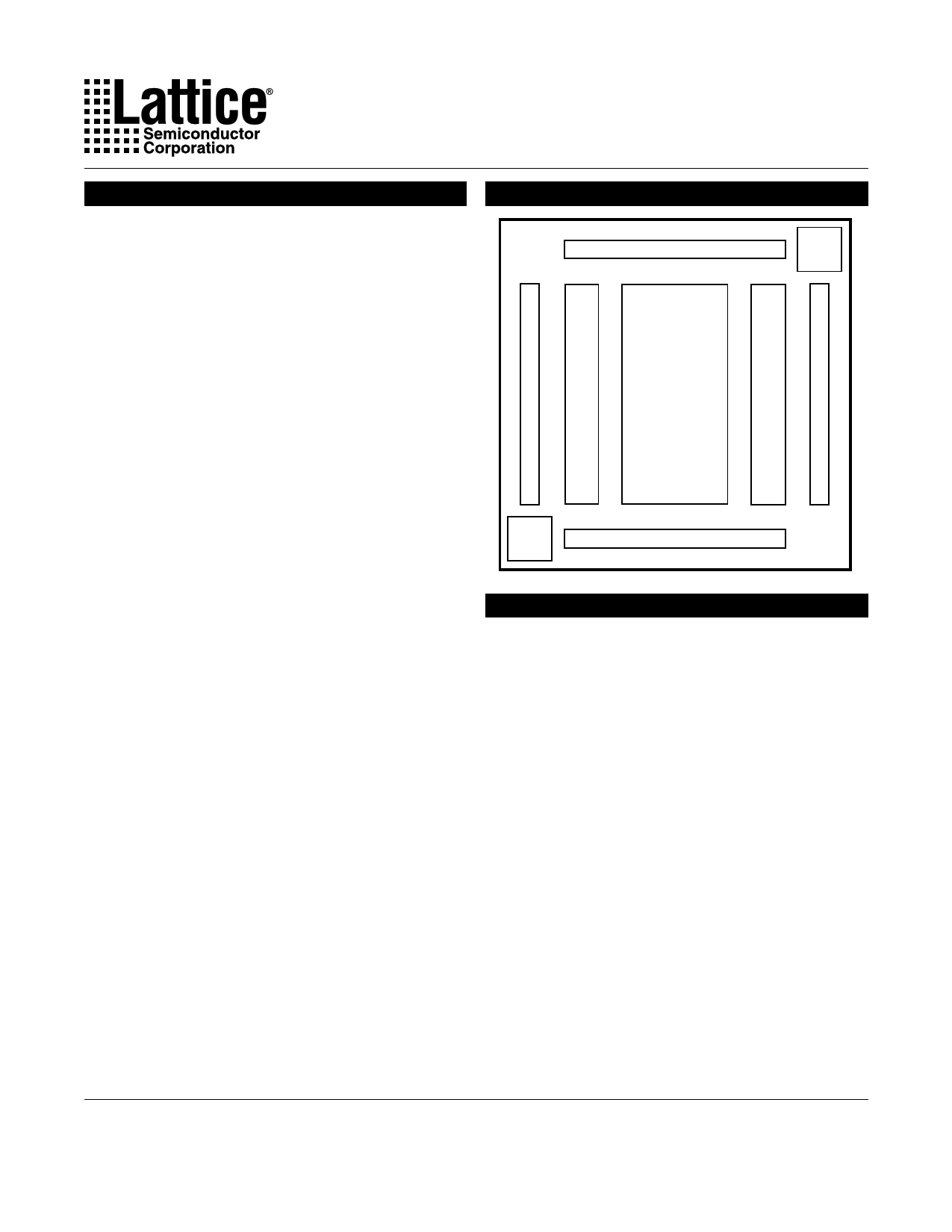
I/O Pins D
ISP
Control
I/O
Cells
Global Routing
Pool
(GRP)
I/O
Cells
Boundary
Scan
Control
I/O Pins B
Description
The ispGDXVA architecture provides a family of fast,
flexible programmable devices to address a variety of
system-level digital signal routing and interface require-
ments including:
• Multi-Port Multiprocessor Interfaces
• Wide Data and Address Bus Multiplexing
(e.g. 16:1 High-Speed Bus MUX)
• Programmable Control Signal Routing
(e.g. Interrupts, DMAREQs, etc.)
• Board-Level PCB Signal Routing for Prototyping or
Programmable Bus Interfaces
The devices feature fast operation, with input-to-output
signal delays (Tpd) of 4.5ns and clock-to-output delays of
4.5ns.
The architecture of the devices consists of a series of
programmable I/O cells interconnected by a Global Rout-
ing Pool (GRP). All I/O pin inputs enter the GRP directly
or are registered or latched so they can be routed to the
required I/O outputs. I/O pin inputs are defined as four
sets (A,B,C,D) which have access to the four MUX inputs
Copyright © 2000 Lattice Semiconductor Corporation. All brand or product names are trademarks or registered trademarks of their respective holders. The specifications and information herein
are subject to change without notice.
LATTICE SEMICONDUCTOR CORP., 5555 Northeast Moore Ct., Hillsboro, Oregon 97124, U.S.A.
Tel. (503) 268-8000; 1-800-LATTICE; FAX (503) 268-8556; http://www.latticesemi.com
September 2000
gdx240va_02
1
1 page 
Specifications ispGDX240VA
Figure 3. Adjacent I/O Cells vs. Direct Input Path for
ispGDX240VA, I/O D33
I/O Group A
D31 MUX Out
I/O Group B
D32 MUX Out
I/O Group C
D34 MUX Out
I/O Group D
D35 MUX Out
ispGDX240VA I/O Cell
4x4
Crossbar
Switch
S1 S0
.m0
.m1
D33
.m2
.m3
It can be seen from Figure 3 that if the D11 adjacent I/O
cell is used, the I/O group “A” input is no longer available
as a direct MUX input.
The ispGDXVA can implement MUXes up to 16 bits wide
in a single level of logic, but care must be taken when
combining adjacent I/O cell outputs with direct MUX
inputs. Any particular combination of adjacent I/O cells as
MUX inputs will dictate what I/O groups (A, B, C or D) can
be routed to the remaining inputs. By properly choosing
the adjacent I/O cells, all of the MUX inputs can be
utilized.
Special Features
Slew Rate Control
All output buffers contain a programmable slew rate
control that provides software-selectable slew rate op-
tions.
Open Drain Control
All output buffers provide a programmable Open-Drain
option which allows the user to drive system level reset,
interrupt and enable/disable lines directly without the
need for an off-chip Open-Drain or Open-Collector buffer.
Wire-OR logic functions can be performed at the printed
circuit board level.
Pull-up Resistor
All pins have a programmable active pull-up. A typical
resistor value for the pull-up ranges from 50kΩ to 80kΩ.
Output Latch (Bus Hold)
All pins have a programmable circuit that weakly holds
the previously driven state when all drivers connected to
the pin (including the pin's output driver as well as any
other devices connected to the pin by external bus) are
tristated.
Table 2. Adjacent I/O Cells (Mapping of
ispGDX240VA)
Data A/ Data B/ Data C/ Data D/
MUXOUT MUXOUT MUXOUT MUXOUT
B30 B32 B31 B29 B28
B31 B33 B32 B30 B29
B32 B34 B33 B31 B30
Reflected B33 B35 B34 B32 B31
I/O Cells D26 D28 D27 D25 D24
D27 D29 D28 D26 D25
D28 D30 D29 D27 D26
D29 D31 D30 D28 D27
D30 D28 D29 D31 D32
D31 D29 D30 D32 D33
D32 D30 D31 D33 D34
Normal D33 D31 D32 D34 D35
I/O Cells
B26 B24 B25 B27 B28
B27 B25 B26 B28 B29
B28 B26 B27 B29 B30
B29 B27 B28 B30 B31
User-Programmable I/Os
The ispGDX240VA features user-programmable
I/Os supporting either 3.3V or 2.5V output voltage level
options. The ispGDX240VA uses a VCCIO pin to provide
the 2.5V reference voltage when used.
PCI Compatible Drive Capability
The ispGDX240VA supports PCI compatible drive capa-
bility for all I/Os.
5
5 Page 
Specifications ispGDX240VA
External Timing Parameters
Over Recommended Operating Conditions
TEST1
PARAMETER COND. #
DESCRIPTION
-4
-7
UNITS
MIN. MAX. MIN. MAX.
tpd2 A 1 Data Prop. Delay from Any I/O pin to Any I/O Pin (4:1 MUX)
– 4.5 – 7.0 ns
tsel2
A 2 Data Prop. Delay from MUXsel Inputs to Any Output (4:1 MUX)
– 4.5 – 7.0 ns
fmax (Tog.) – 3 Clock Frequency, Max. Toggle
200 – 100 – MHz
fmax (Ext.)
–
4
Clock Frequency with External Feedback (
1
tsu3+tgco1
)
111 – 80 – MHz
tsu1
tsu2
– 5 Input Latch or Register Setup Time Before Yx
– 6 Input Latch or Register Setup Time Before I/O Clock
4.0 –
3.0 –
5.5 –
4.5 –
ns
ns
tsu3
tsu4
– 7 Output Latch or Register Setup Time Before Yx
– 8 Output Latch or Register Setup Time Before I/O Clock
4.0 –
3.0 –
5.5 –
4.5 –
ns
ns
tsuce1
tsuce2
– 9 Global Clock Enable Setup Time Before Yx
– 10 Global Clock Enable Setup Time Before I/O Clock
2.5 –
1.5 –
3.5 –
2.5 –
ns
ns
tsuce3
th1
th2
– 11 I/O Clock Enable Setup Time Before Yx
– 12 Input Latch or Reg. Hold Time (Yx)
– 13 Input Latch or Reg. Hold Time (I/O Clock)
4.5 –
0.0 –
1.5 –
6.5 –
0.0 –
2.5 –
ns
ns
ns
th3 – 14 Output Latch or Reg. Hold Time (Yx)
th4 – 15 Output Latch or Reg. Hold Time (I/O Clock)
0.0 –
1.5 –
0.0 –
2.5 –
ns
ns
thce1
thce2
– 16 Global Clock Enable Hold Time (Yx)
– 17 Global Clock Enable Hold Time (I/O Clock)
0.0 –
1.5 –
0.0 –
2.5 –
ns
ns
thce3
tgco12
tgco22
tco12
– 18 I/O Clock Enable Hold Time (Yx)
A 19 Output Latch or Reg. Clock (from Yx) to Output Delay
A 20 Input Latch or Register Clock (from Yx) to Output Delay
A 21 Output Latch or Register Clock (from I/O pin) to Output Delay
0.0 –
– 4.5
– 8.5
– 6.0
0.0 –
– 7.0
– 11.0
– 9.0
ns
ns
ns
ns
tco22
A 22 Input Latch or Register Clock (from I/O pin) to Output Delay
– 9.5 – 13.0 ns
ten2 B 23 Input to Output Enable
– 6.0 – 8.5 ns
tdis2
C 24 Input to Output Disable
– 6.0 – 8.5 ns
ttoeen2
B 25 Test OE Output Enable
– 7.0 – 8.5 ns
ttoedis2
C 26 Test OE Output Disable
– 7.0 – 8.5 ns
twh – 27 Clock Pulse Duration, High
3.5 – 5.0 – ns
twl – 28 Clock Pulse Duration, Low
3.5 – 5.0 – ns
trst – 29 Register Reset Delay from RESET Low
– 14.0 – 18.0 ns
trw – 30 Reset Pulse Width
10.0 – 14.0 – ns
tsl
D 31 Output Delay Adder for Output Timings Using Slow Slew Rate
– 4.5 – 7.0 ns
tsk A 32 Output Skew (tgco1 Across Chip)
– 0.5 – 0.5 ns
1. All timings measured with one output switching, fast output slew rate setting, except tsl.
2. The delay parameters are measured with Vcc as I/O voltage reference. An additional 0.5ns delay is incurred when Vccio is
used as I/O voltage reference.
11
11 Page | ||
| Páginas | Total 25 Páginas | |
| PDF Descargar | [ Datasheet 240VA.PDF ] | |
Hoja de datos destacado
| Número de pieza | Descripción | Fabricantes |
| 240VA | In-SystemProgrammable3.3VGenericDigitalCrosspointTM | LatticeSemiconductor |
| Número de pieza | Descripción | Fabricantes |
| SLA6805M | High Voltage 3 phase Motor Driver IC. |
Sanken |
| SDC1742 | 12- and 14-Bit Hybrid Synchro / Resolver-to-Digital Converters. |
Analog Devices |
|
DataSheet.es es una pagina web que funciona como un repositorio de manuales o hoja de datos de muchos de los productos más populares, |
| DataSheet.es | 2020 | Privacy Policy | Contacto | Buscar |