|
|
|
PDF FSD200B Data sheet ( Hoja de datos )
| Número de pieza | FSD200B | |
| Descripción | Green Mode Fairchild Power Switch | |
| Fabricantes | Fairchild Semiconductor | |
| Logotipo | ||
Hay una vista previa y un enlace de descarga de FSD200B (archivo pdf) en la parte inferior de esta página. Total 18 Páginas | ||
|
No Preview Available !
www.fairchildsemi.com
FSD210B, FSD200B
Green Mode Fairchild Power Switch (FPSTM)
Features
• Single Chip 700V Sense FET Power Switch for 7DIP
• Precision Fixed Operating Frequency (134KHz)
• FSD210B Consumes Under 0.1W at 265VAC & No Load
with Advanced Burst-Mode Operation
• Internal Start-up Circuit
• Pulse-by-Pulse Current Limiting
• Over Load Protection (OLP)
• Internal Thermal Shutdown Function (TSD)
• Auto-Restart Mode
• Under Voltage Lockout (UVLO) with Hysteresis
• Built-in Soft Start
• Frequency Modultation for EMI Reduction
• FSD200B Does Not Require an Auxiliary Bias Winding
Applications
• Charger & Adapter for Mobile Phone, PDA & MP3
• Auxiliary Power for White Goods, PC, C-TV & Monitor
PRODUCT
FSD210B
FSD200B
FSD210BM
FSD200BM
OUTPUT POWER TABLE
230VAC ±15%(3)
85-265VAC
Adapter(1)
Open
Frame(2)
Adapter(1)
Open
Frame(2)
5W 7W 4W 5W
5W 7W 4W 5W
5W 7W 4W 5W
5W 7W 4W 5W
Notes:
1. T ypical continuo us power in a non-ventilated enclosed
adapter with sufficient drain pattern as a heat s inker, a t
50°C ambient.
2. Maximum practical con tinuous power in an open frame
design with sufficient drain pattern as a heat sinker, at 50°C
ambient.
3. 230 VAC or 100/115 VAC with doubler.
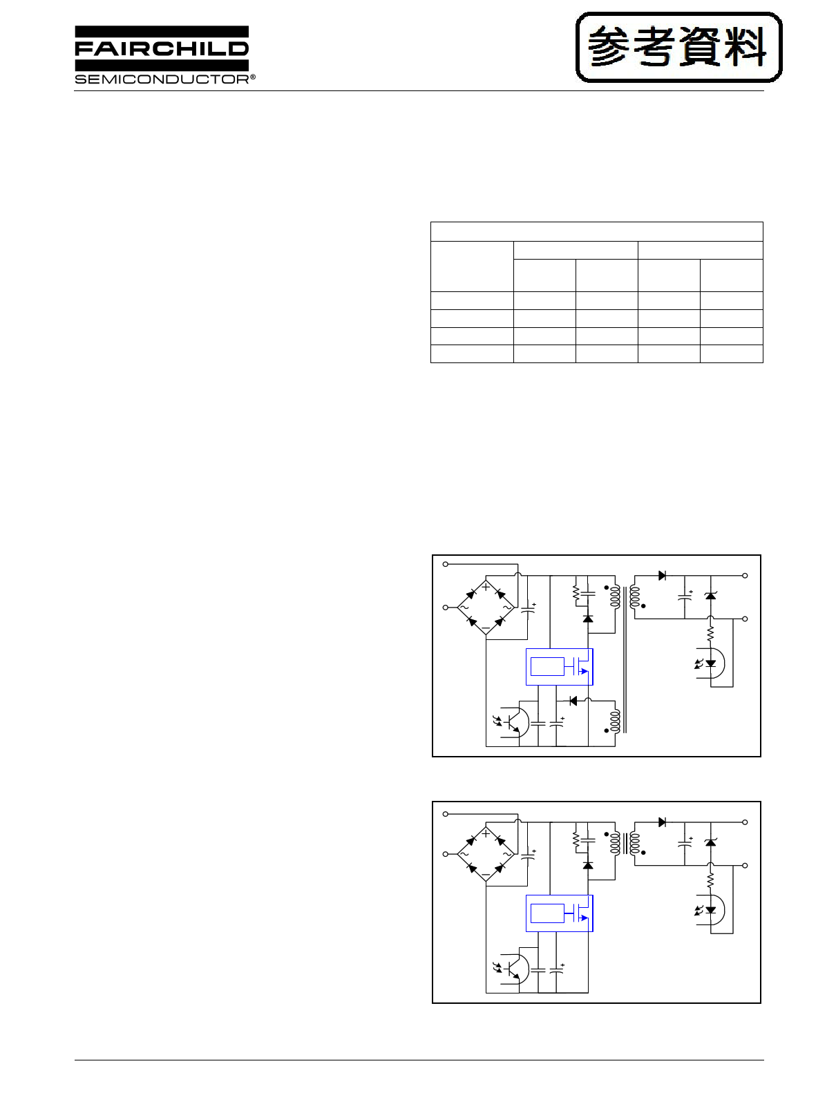
Typical Circuit
Related Application Notes
• AN-4137, 4141, 4147(Flyback) / AN-4134(Forward) /
AN-4138(Charger)
Description
Each product in the FSD2x0B (x for 0, 1) family c onsists of
an integrated Pulse Width Modulator (PWM) a nd Se nse
FET, and is specifically designed for high perform ance off-
line Switch Mode Power Su pplies (SMPS) with minimal
external components. Both dev ices are integrated high volt-
age power switching regulators which combine an avalanche
rugged Sense FET with a voltage mode PWM control block.
The in tegrated PWM c ontroller features inc lude: a fixed
oscillator with freque ncy modulation for red uced EMI,
Under Voltage Lock Out (UVLO) protection, Leading Edge
Blanking (LEB), an o ptimized gate turn-on/turn-off drive r,
Thermal Shut Down (TSD) protection and temperature com-
pensated prec ision current source s for lo op co mpensation
and fault protection circuitry. When compared to a discrete
MOSFET and controller or RCC switching conv erter solu-
tion, the FSD2x0B de vices reduc e total component c ount,
design size, weight while increasing efficiency, productivity,
and system reliability. Both devices provide a basic platform
that is well suited fo r the design of cost-ef fective flyback
converters.
FPSTM is a trademark of Fairchild Semiconductor Corporation.
©2005 Fairchild Semiconductor Corporation
AC
IN
Vstr Drain
PWM
Vfb Vcc Source
DC
OUT
Figure 1. Typical Flyback Application for FSD210B
AC
IN
Vstr Drain
PWM
Vfb Vcc Source
DC
OUT
Figure 2. Typical Flyback Application for FSD200B
Rev.1.0.3
http://www.Datasheet4U.com
1 page 
FSD210B, FSD200B
Electrical Characteristics
(Ta = 25°C unless otherwise specified)
Parameter Sym
bol
Condition
Min. Typ. Max.
SENSE FET SECTION
Zero-Gate-Voltage Drain Current
IDSS VDS=560V, VGS=0V -
- 100
Drain-Source On-State Resistance
RDS(ON)
Tj=25°C, ID=25mA -
Tj=100°C, ID=25mA -
28 32
42 48
Rise Time
tr VDS=325V, ID=50mA
- 100 -
Fall Time
tf VDS=325V, ID=25mA
- 50 -
CONTROL SECTION
Switching Frequency
fOSC Tj =25°C
126 134
142
Switching Frequency Modulation Range ∆fMOD Tj=25°C-
±4 -
Maximum Duty Cycle
DMAX VFB=3.5V
60 66
72
Minimum Duty Cycle
DMIN VFB=GND
00 0
UVLO Threshold Voltage (FSD200B)
VSTART 6.3
VSTOP After turn on
7 7.7
5.3 6 6.7
UVLO Threshold Voltage (FSD210B)
VSTART 8.0
VSTOP After turn on
8.7 9.4
6.0 6.7 7.4
Feedback Source Current
IFB V FB=GND 0.22
0.25 0.28
Internal Soft Start Time
tS/S -
3-
BURST MODE SECTION
Burst Mode Voltage
VBURH
VBURL
Tj=25°C
0.58 0.64 0.7
0.5 0.58
0.64
VBUR(HYS) Hysteresis
- 60 -
PROTECTION SECTION
Peak Current Limit
Current Limit Delay Time(1)
Thermal Shutdown Temperature(1)
ILIM ∆i/∆t=150mA/us
tCLD Tj=25°C
TSD 125
0.275 0.320
- 220
145
0.365
-
160
Shutdown Feedback Voltage
Leading Edge Blanking Time(2)
VSD 4.0
tLEB 200
4.5 5.0
--
Shutdown Delay Current
TOTAL DEVICE SECTION
IDELAY VFB=4.0V
35 7
Operating Supply Current (FSD200B)
IOP (control part only),VCC=7V - 600
-
Start-Up Charging Current (FSD200B)
ICH V CC=0V
- 1 1.2
Operating Supply Current (FSD210B)
IOP (control part only),VCC=11V - 700
-
Start-Up Charging Current (FSD210B)
ICH V CC=0V
- 700 900
Vstr Supply Voltage
VSTR V CC=0V
20 -
-
Vcc Regulation Voltage (FSD200B)
VCCREG -7
-
Unit
µA
Ω
ns
ns
KHz
KHz
%
%
V
V
V
V
mA
ms
V
V
mV
A
ns
°C
V
ns
µA
µA
mA
µA
µA
V
V
Note:
1. These parameters, although guaranteed, are not 100% tested in production
2. These parameter is derived from characterization
5
5 Page 
FSD210B, FSD200B
6. Burst operation : In order to minimize the power dissi-
pation in standby mode, the FSD200B/210B enter burst
mode operation. As the load decreases, the feedback voltage
decreases. The device automatically enters burst mode when
the fe edback voltage dro ps below V BURL(0.58V). At this
point switching st ops and the output voltages start to drop.
This ca use s th e fee dback vo ltag e to rise. Onc e is pa sses
VBURH(0.64V) switching starts again. The feedback voltage
falls and the process repea ts. Burst mode operation alter-
nately enables and disables switching of the power MOSFET
to reduce the switching loss in the standby mode.
Vo
Voset
fs=1/ts
138kHz
134kHz
130kHz
Drain
Current
ts
4ms t
Figure 13. Frequency Modulation Waveform
VFB
0.64V
0.58V
Ids
CISPR22Q(PK)
CISPR22A(AV)
Vds
t
4
Vfb
5uA
OSC
250uA
SQ
R
GATE
DRIVER
on/off
0.64V
/0.58V
FSD2xxB
Burst Operation Block
Figure 12. Burst Operation Function
Frequency(MHz)
Figure 14. FSDH0165 Full Range EMI scan(100kHz, no
Frequency Modulation) with charger set
CISPR22Q(PK)
CISPR22A(AV)
7. Frequency Modulation : Modulatin g the switc hing fre-
quency of a sw itched power su pply can reduce EMI by
spreading the energy over a wide r frequency range than the
bandwidth measured b y the EMI test e quipment. The
amount of EMI reduc tion is direc tly related to the depth of
the reference frequency. As can be seen in Figure 13, the fre-
quency c hanges from 130K Hz to 138KH z in 4 ms for the
FSD200B/210B. Frequency modulation allows the use of a
cost effective inductor instead of an AC input mode choke to
satisfy the requirements of world wide EMI limits.
Frequency(MHz)
Figure 15. FSD210B Full Range EMI scan(134kHz, with
Frequency Modulation) with charger set
11
11 Page | ||
| Páginas | Total 18 Páginas | |
| PDF Descargar | [ Datasheet FSD200B.PDF ] | |
Hoja de datos destacado
| Número de pieza | Descripción | Fabricantes |
| FSD200 | Green Mode Fairchild Power Switch (FPSTM) | Fairchild Semiconductor |
| FSD200B | Green Mode Fairchild Power Switch | Fairchild Semiconductor |
| FSD200M | Green Mode Fairchild Power Switch (FPSTM) | Fairchild Semiconductor |
| Número de pieza | Descripción | Fabricantes |
| SLA6805M | High Voltage 3 phase Motor Driver IC. |
Sanken |
| SDC1742 | 12- and 14-Bit Hybrid Synchro / Resolver-to-Digital Converters. |
Analog Devices |
|
DataSheet.es es una pagina web que funciona como un repositorio de manuales o hoja de datos de muchos de los productos más populares, |
| DataSheet.es | 2020 | Privacy Policy | Contacto | Buscar |