|
|
|
PDF LT6109-1 Data sheet ( Hoja de datos )
| Número de pieza | LT6109-1 | |
| Descripción | (LT6109-1/-2) High Side Current Sense Amplifier | |
| Fabricantes | Linear Technology | |
| Logotipo | ||
Hay una vista previa y un enlace de descarga de LT6109-1 (archivo pdf) en la parte inferior de esta página. Total 28 Páginas | ||
|
No Preview Available !
FEATURES
n Current Sense Amplifier
– Fast Step Response: 500ns
– Low Offset Voltage: 125µV Maximum
– Low Gain Error: 0.2% Maximum
n Internal 400mV Precision Reference
n Internal Latching Comparators with Reset
– Fast Response Time: 500ns
– Total Threshold Error: ±1.25% Maximum
– Two Comparator Polarity Options
n Wide Supply Range: 2.7V to 60V
n Supply Current: 550µA
n Low Shutdown Current: 5µA Maximum
n Specified for –40°C to 125°C Temperature Range
n Available in 10-Lead MSOP Package
APPLICATIONS
n Overcurrent, Undercurrent and Fault Detection
n Current Shunt Measurement
n Battery Monitoring
n Motor Control
n Automotive Monitoring and Control
n Remote Sensing
n Industrial Control
LT6109-1/LT6109-2
High Side Current Sense
Amplifier with Reference
and Comparators
DESCRIPTION
The LT®6109 is a complete high side current sense device
that incorporates a precision current sense amplifier, an
integrated voltage reference and two comparators. Two
versions of the LT6109 are available. The LT6109-1 has
the comparators connected in opposing polarity and the
LT6109-2 has the comparators connected in the same polar-
ity. In addition, the current sense amplifier and comparator
inputs and outputs are directly accessible. The amplifier
gain and comparator trip points are configured by external
resistors. The open-drain comparator outputs allows for
easy interface to other system components.
The overall propagation delay of the LT6109 is typically
only 1.4µs, allowing for quick reaction to overcurrent
and undercurrent conditions. The 1MHz bandwidth al-
lows the LT6109 to be used for error detection in critical
applications such as motor control. The high threshold
accuracy of the comparators, combined with the ability to
latch both comparators, ensures the LT6109 can capture
high speed events.
The LT6109 is fully specified for operation from –40°C to
125°C, making it suitable for industrial and automotive ap-
plications. The LT6109 is available in a small 10-lead MSOP.
L, LT, LTC, LTM, TimerBlox, Linear Technology and the Linear logo are registered trademarks
of Linear Technology Corporation. All other trademarks are the property of their respective
owners.
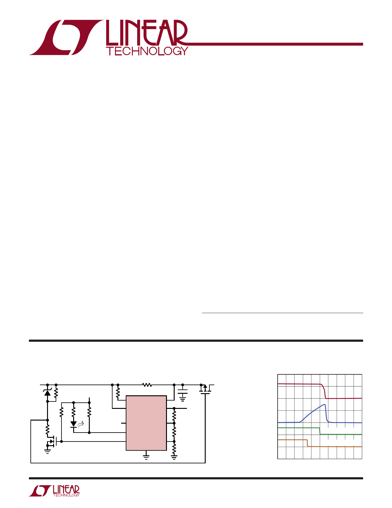
TYPICAL APPLICATION
Circuit Fault Protection with Latching Load Disconnect and Early Warning Indication
12V
6.2V*
1k
10k
1k
2N2700
0.1Ω
3.3V
1.62k 100k
100Ω
SENSEHI SENSELO
V+ OUTA
LT6109-2
RESET EN/RST
100mA WARNING OUTC2
250mA DISCONNECT OUTC1 V–
INC2
INC1
IRF9640
TO LOAD
0.1µF
VOUT
6.04k
2.37k
1.6k
*CMH25234B
610912 TA01a
Response to Overcurrent Event
VLOAD
10V/DIV
0V
ILOAD
200mA/DIV
0mA
VOUTC1
5V/DIV 0V
VOUTC2
5V/DIV 0V
250mA DISCONNECT
100mA WARNING
5µs/DIV
610912 TA01b
610912fa
1
Free Datasheet http://www.Datasheet4U.com
1 page 
LT6109-1/LT6109-2
TYPICAL PERFORMANCE CHARACTERISTICS
V+
=
12V,
VPULLUP
=
V+,
VEN/RST
=
2.7V,
RIN
=
100Ω,
ROUT
=
R1
+
R2
+
R3
=
10k,
Performance characteristics taken at
gain = 100, RC = 25.5k, CL = CLC = 2pF,
uTnAle=s2s5°C,
otherwise noted. (See Figure 3)
Supply Current vs Supply Voltage
700
Start-Up Supply Current
600
V+
500 5V/DIV
0V
400
300
IS
200 500µA/DIV
100
0
0
10 20 30 40 50 60
SUPPLY VOLTAGE (V)
610912 G01
0µA
10µs/DIV
Enable/Disable Response
VEN/RST
2V/DIV
0V
IS
500µA/DIV
0µA
610912 G02
100µs/DIV
610912 G03
Input Offset Voltage
vs Temperature
300
5 TYPICAL UNITS
200
100
0
–100
–200
–300
–40 –25 –10 5 20 35 50 65 80 95 110 125
TEMPERATURE (°C)
610912 G04
Amplifier Gain Error
vs Temperature
0.05 VSENSE = 5mV TO 100mV
0
–0.05
–0.10
RIN = 1k
RIN = 100Ω
–0.15
–0.20
–50 –25
0 25 50 75
TEMPERATURE (°C)
100 125
610912 G07
Amplifier Offset Voltage
vs Supply Voltage
100 5 TYPICAL UNITS
80
60
40
20
0
–20
–40
–60
–80
–100
0
10 20 30 40
SUPPLY VOLTAGE (V)
50 60
610912 G05
Amplifier Gain Error Distribution
25 VSENSE = 5mV TO 100mV
20
15
10
5
0
–0.048 –0.052 –0.056 –0.060 –0.064 –0.68
GAIN ERROR (%)
610912 G08
Offset Voltage Drift Distribution
12
10
8
6
4
2
0
–2 –1.5 –1 –0.5 0 0.5 1 1.5 2
OFFSET VOLTAGE DRIFT (µV/°C)
610912 G06
Amplifier Output Swing
vs Temperature
0.50
0.45
0.40 V+ = 12V
0.35 VSENSE = 120mV
0.30
0.25
0.20
0.15 V+ = 2.7V
0.10 VSENSE = 27mV
0.05
0
–50 –25
0 25 50 75
TEMPERATURE (°C)
100 125
610912 G18
610912fa
5
Free Datasheet http://www.Datasheet4U.com
5 Page 
LT6109-1/LT6109-2
APPLICATIONS INFORMATION
The output current can be transformed back into a voltage
by adding a resistor from OUTA to V–(typically ground).
The output voltage is then:
VOUT = V– + IOUTA • ROUT
where ROUT = R1 + R2 + R3 as shown in Figure 3.
Table 1. Example Gain Configurations
GAIN RIN ROUT VSENSE FOR VOUT = 5V
20 499Ω 10k
250mV
50 200Ω 10k
100mV
100 100Ω 10k
50mV
IOUTA AT VOUT = 5V
500µA
500µA
500µA
Useful Equations
Input Voltage: VSENSE = ISENSE •RSENSE
Voltage Gain:
VOUT
VSENSE
=
ROUT
RIN
Current Gain:
IOUTA
ISENSE
=
RSENSE
RIN
Note that VSENSE(MAX) can be exceeded without damag-
ing the amplifier, however, output accuracy will degrade
as VSENSE exceeds VSENSE(MAX), resulting in increased
output current, IOUTA.
Selection of External Current Sense Resistor
The external sense resistor, RSENSE, has a significant effect
on the function of a current sensing system and must be
chosen with care.
First, the power dissipation in the resistor should be
considered. The measured load current will cause power
dissipation as well as a voltage drop in RSENSE. As a
result, the sense resistor should be as small as possible
while still providing the input dynamic range required by
the measurement. Note that the input dynamic range is
the difference between the maximum input signal and the
minimum accurately reproduced signal, and is limited
primarily by input DC offset of the internal sense ampli-
fier of the LT6109. To ensure the specified performance,
RSENSE should be small enough that VSENSE does not
exceed VSENSE(MAX) under peak load conditions. As an
example, an application may require the maximum sense
voltage be 100mV. If this application is expected to draw
2A at peak load, RSENSE should be set to 50mΩ.
Once the maximum RSENSE value is determined, the mini-
mum sense resistor value will be set by the resolution or
dynamic range required. The minimum signal that can be
accurately represented by this sense amplifier is limited by
the input offset. As an example, the LT6109 has a maximum
input offset of 125µV. If the minimum current is 20mA, a
sense resistor of 6.25mΩ will set VSENSE to 125µV. This is
the same value as the input offset. A larger sense resistor
will reduce the error due to offset by increasing the sense
voltage for a given load current. Choosing a 50mΩ RSENSE
will maximize the dynamic range and provide a system
that has 100mV across the sense resistor at peak load
(2A), while input offset causes an error equivalent to only
2.5mA of load current.
In the previous example, the peak dissipation in RSENSE
is 200mW. If a 5mΩ sense resistor is employed, then
the effective current error is 25mA, while the peak sense
voltage is reduced to 10mV at 2A, dissipating only 20mW.
The low offset and corresponding large dynamic range of
the LT6109 make it more flexible than other solutions in this
respect. The 125µV maximum offset gives 72dB of dynamic
range for a sense voltage that is limited to 500mV max.
Sense Resistor Connection
Kelvin connection of the SENSEHI and SENSELO inputs
to the sense resistor should be used in all but the lowest
power applications. Solder connections and PC board
interconnections that carry high currents can cause sig-
nificant error in measurement due to their relatively large
resistances. One 10mm × 10mm square trace of 1oz copper
is approximately 0.5mΩ. A 1mV error can be caused by as
little as 2A flowing through this small interconnect. This
will cause a 1% error for a full-scale VSENSE of 100mV.
A 10A load current in the same interconnect will cause
a 5% error for the same 100mV signal. By isolating the
sense traces from the high current paths, this error can
be reduced by orders of magnitude. A sense resistor with
integrated Kelvin sense terminals will give the best results.
Figure 3 illustrates the recommended method for connect-
ing the SENSEHI and SENSELO pins to the sense resistor.
610912fa
11
Free Datasheet http://www.Datasheet4U.com
11 Page | ||
| Páginas | Total 28 Páginas | |
| PDF Descargar | [ Datasheet LT6109-1.PDF ] | |
Hoja de datos destacado
| Número de pieza | Descripción | Fabricantes |
| LT6109-1 | (LT6109-1/-2) High Side Current Sense Amplifier | Linear Technology |
| LT6109-2 | (LT6109-1/-2) High Side Current Sense Amplifier | Linear Technology |
| Número de pieza | Descripción | Fabricantes |
| SLA6805M | High Voltage 3 phase Motor Driver IC. |
Sanken |
| SDC1742 | 12- and 14-Bit Hybrid Synchro / Resolver-to-Digital Converters. |
Analog Devices |
|
DataSheet.es es una pagina web que funciona como un repositorio de manuales o hoja de datos de muchos de los productos más populares, |
| DataSheet.es | 2020 | Privacy Policy | Contacto | Buscar |