|
|
|
PDF SA572 Data sheet ( Hoja de datos )
| Número de pieza | SA572 | |
| Descripción | Programmable analog compandor | |
| Fabricantes | Philips | |
| Logotipo | ||
Hay una vista previa y un enlace de descarga de SA572 (archivo pdf) en la parte inferior de esta página. Total 8 Páginas | ||
|
No Preview Available !
Philips Semiconductors RF Communications Products
Programmable analog compandor
Product specification
NE/SA572
DESCRIPTION
The NE572 is a dual-channel,
high-performance gain control circuit in which
either channel may be used for dynamic
range compression or expansion. Each
channel has a full-wave rectifier to detect the
average value of input signal, a linearized,
temperature-compensated variable gain cell
(∆G) and a dynamic time constant buffer. The
buffer permits independent control of
dynamic attack and recovery time with
minimum external components and improved
low frequency gain control ripple distortion
over previous compandors.
The NE572 is intended for noise reduction in
high-performance audio systems. It can also
be used in a wide range of communication
systems and video recording applications.
FEATURES
• Independent control of attack and recovery
time
• Improved low frequency gain control ripple
• Complementary gain compression and
expansion with external op amp
• Wide dynamic range—greater than 110dB
• Temperature-compensated gain control
• Low distortion gain cell
• Low noise—6µV typical
• Wide supply voltage range—6V-22V
• System level adjustable with external
components
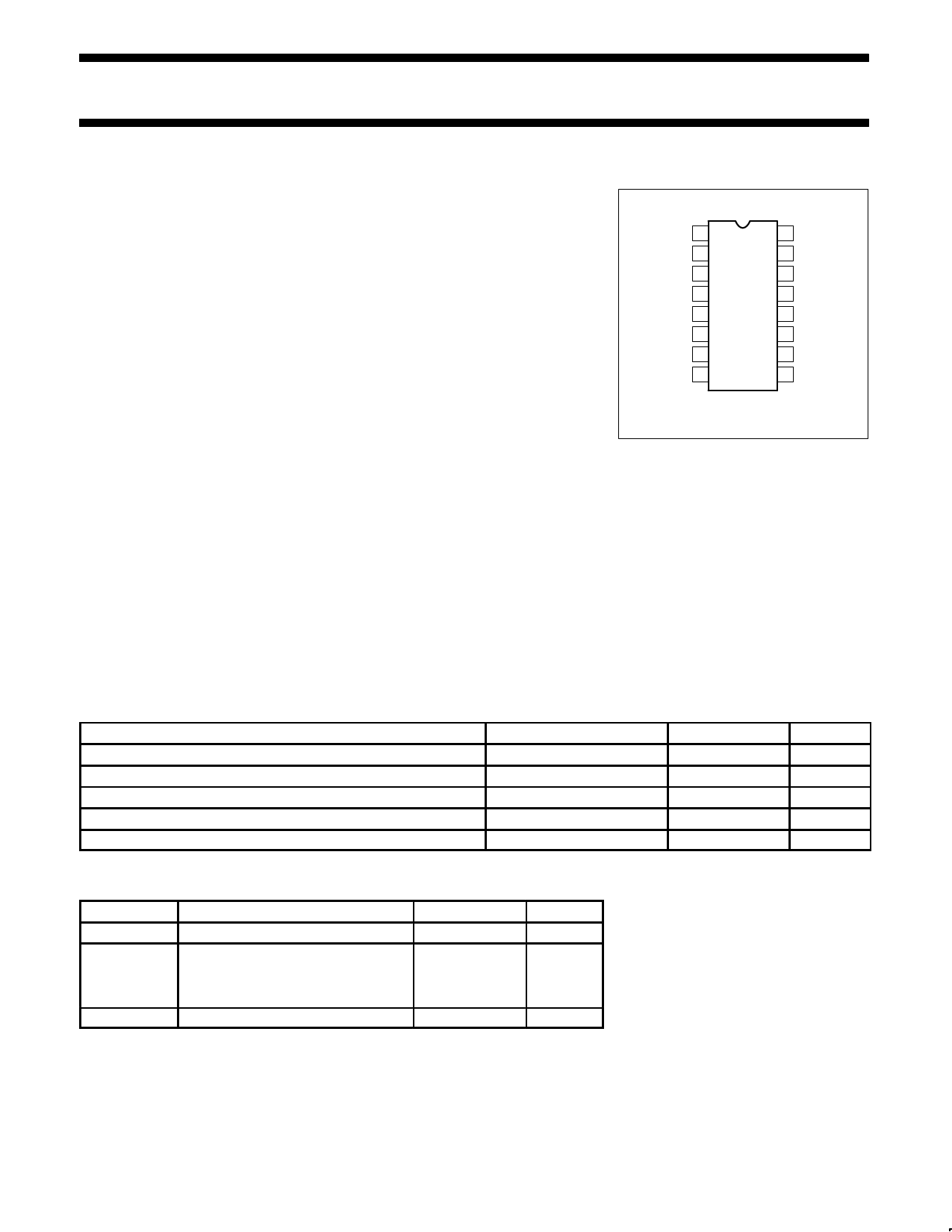
PIN CONFIGURATION
D1, N, F Packages
TRACK TRIM A 1
RECOV. CAP A 2
RECT. IN A 3
ATTACK CAP A 4
∆G OUT A 5
THD TRIM A 6
∆G IN A 7
GND 8
16 VCC
15 TRACK TRIM B
14 RECOV. CAP B
13 RECT. IN B
12 ATTACK CAP B
11 ∆G OUT B
10 THD TRIM B
9 ∆G IN B
NOTE:
1. D package released in large SO (SOL) package
only.
APPLICATIONS
• Dynamic noise reduction system
• Voltage control amplifier
• Stereo expandor
• Automatic level control
• High-level limiter
• Low-level noise gate
• State variable filter
ORDERING INFORMATION
DESCRIPTION
16-Pin Plastic Small Outline (SO)
16-Pin Plastic Dual In-Line Package (DIP)
16-Pin Plastic Small Outline (SO)
16-Pin Ceramic Dual In-Line Package (Cerdip)
16-Pin Plastic Dual In-Line Package (DIP)
TEMPERATURE RANGE
0 to +70°C
0 to +70°C
–40 to +85°C
–40 to +85°C
–40 to +85°C
ORDER CODE
NE572D
NE572N
SA572D
SA572F
SA572N
DWG #
0005
0406
0005
0582
0406
ABSOLUTE MAXIMUM RATINGS
SYMBOL
PARAMETER
VCC Supply voltage
TA Operating temperature range
NE572
SA572
PD Power dissipation
RATING
22
0 to +70
–40 to +85
500
UNIT
VDC
°C
mW
October 7, 1987
2 853-0813 90829
Free Datasheet http://www.datasheet4u.com/
1 page 
Philips Semiconductors RF Communications Products
Programmable analog compandor
Product specification
NE/SA572
VREF
+
A2
–
R2
VIN
V+
IR
+
VIN *
VREF
R2
Q5
Q6
D7
Figure 2. Simplified Rectifier Schematic
Q8 Q9
V+
Q10
Q17
IR
+
VIN
R
10k
–
A3
+
IR1
D11
D12
IQ = 2IR2
IR2
10k
D15
D13
X2
Q16
Q14
X2
Q18
CR
CA TRACKING
TRIM
Figure 3. Buffer Amplifier Schematic
Buffer Amplifier
In audio systems, it is desirable to have fast
attack time and slow recovery time for a tone
burst input. The fast attack time reduces
transient channel overload but also causes
low-frequency ripple distortion. The
low-frequency ripple distortion can be
improved with the slow recovery time. If
different attack times are implemented in
corresponding frequency spectrums in a split
band audio system, high quality performance
can be achieved. The buffer amplifier is
designed to make this feature available with
minimum external components. Referring to
Figure 3, the rectifier output current is
mirrored into the input and output of the
unipolar buffer amplifier A3 through Q8, Q9
and Q10. Diodes D11 and D12 improve
tracking accuracy and provide
common-mode bias for A3. For a
positive-going input signal, the buffer
amplifier acts like a voltage-follower.
Therefore, the output impedance of A3 makes
the contribution of capacitor CR to attack time
insignificant. Neglecting diode impedance,
the gain Ga(t) for ∆G can be expressed as
follows:
*t
Ga(t) + (GaINT * GaFNL e t A ) GaFNL
GaINT=Initial Gain
GaFNL=Final Gain
τA=RA • CA=10k • CA
where τA is the attack time constant and RA
is a 10k internal resistor. Diode D15 opens
the feedback loop of A3 for a negative-going
signal if the value of capacitor CR is larger
than capacitor CA. The recovery time
depends only on CR • RR. If the diode
impedance is assumed negligible, the
dynamic gain GR (t) for ∆G is expressed as
follows.
*t
GR(t) + (GRINT * GRFNL et R ) GRFNL
GR(t)=(GR INT–GR FNL) e +GR FNL
τR=RR • CR=10k • CR
where τR is the recovery time constant and
RR is a 10k internal resistor. The gain control
current is mirrored to the gain cell through
Q14. The low level gain errors due to input
bias current of A2 and A3 can be trimmed
through the tracking trim pin into A3 with a
current source of ±3µA.
Basic Expandor
Figure 4 shows an application of the circuit as
a simple expandor. The gain expression of
the system is given by
October 7, 1987
6
Free Datasheet http://www.datasheet4u.com/
5 Page | ||
| Páginas | Total 8 Páginas | |
| PDF Descargar | [ Datasheet SA572.PDF ] | |
Hoja de datos destacado
| Número de pieza | Descripción | Fabricantes |
| SA57000-25D | CapFREE 150 mA / low-noise / low dropout regulator with thermal protection | Philips |
| SA57000-28D | CapFREE 150 mA / low-noise / low dropout regulator with thermal protection | Philips |
| SA57000-30D | CapFREE 150 mA / low-noise / low dropout regulator with thermal protection | Philips |
| SA57000-33D | CapFREE 150 mA / low-noise / low dropout regulator with thermal protection | Philips |
| Número de pieza | Descripción | Fabricantes |
| SLA6805M | High Voltage 3 phase Motor Driver IC. |
Sanken |
| SDC1742 | 12- and 14-Bit Hybrid Synchro / Resolver-to-Digital Converters. |
Analog Devices |
|
DataSheet.es es una pagina web que funciona como un repositorio de manuales o hoja de datos de muchos de los productos más populares, |
| DataSheet.es | 2020 | Privacy Policy | Contacto | Buscar |