|
|
|
PDF ZL9117M Data sheet ( Hoja de datos )
| Número de pieza | ZL9117M | |
| Descripción | Digital DC/DC PMBus 17A Module | |
| Fabricantes | Intersil | |
| Logotipo | ||
Hay una vista previa y un enlace de descarga de ZL9117M (archivo pdf) en la parte inferior de esta página. Total 17 Páginas | ||
|
No Preview Available !
Digital DC/DC PMBus 17A Module
ZL9117M
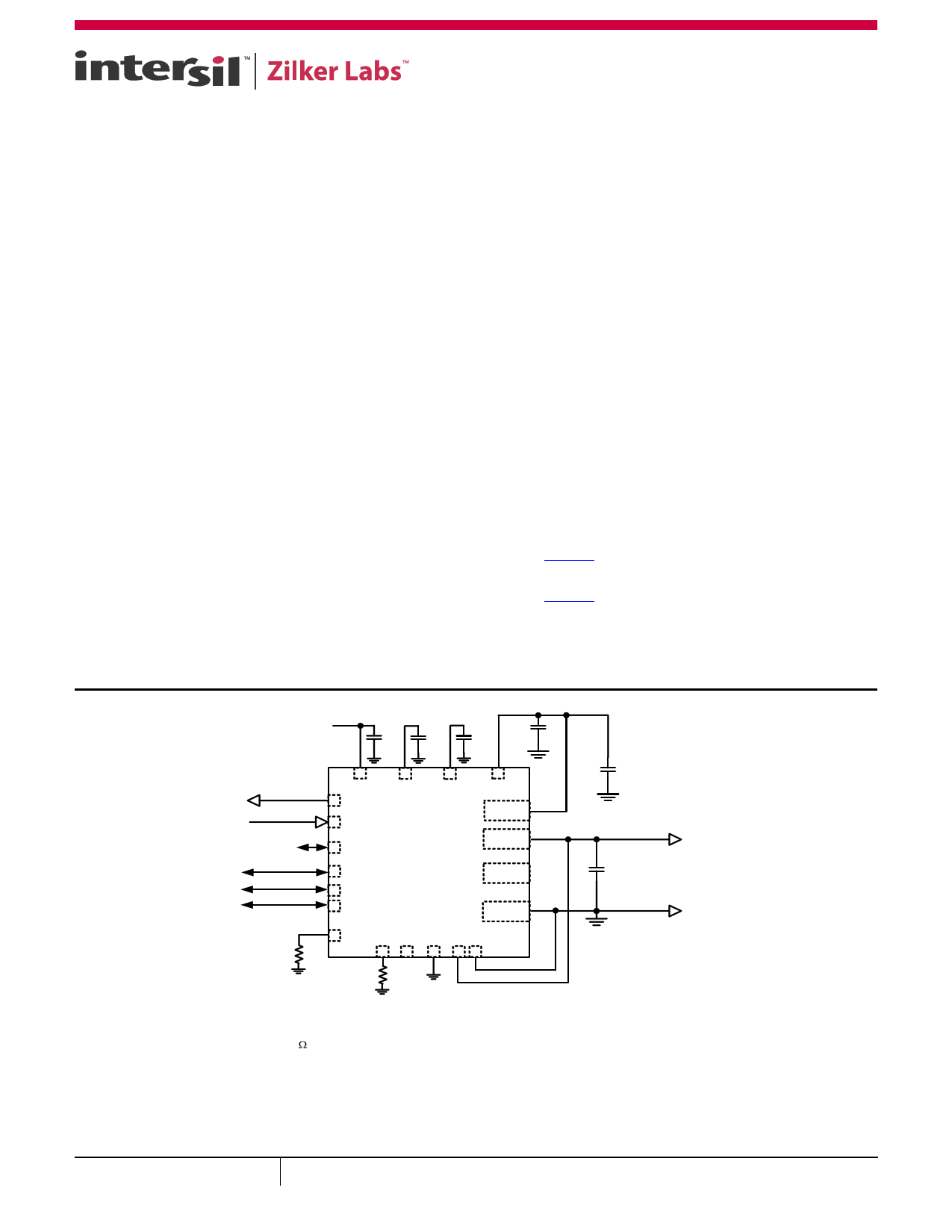
The ZL9117M is a 17A, variable output, step-down
PMBus-compliant digital power supply. Included in the module
is a high-performance digital PWM controller, power MOSFETs,
an inductor, and all the passive components required for a
highly integrated DC/DC power solution. This power module
has built-in auto-compensation algorithms, which eliminates
the need for manual compensation design work. The ZL9117M
operates over a wide input voltage range and supports an
output voltage range of 0.6V to 3.6V, which can be set by
external resistors or via PMBus. This high-efficiency power
module is capable of delivering 17A. Only bulk input and
output capacitors are needed to finish the design. The output
voltage can be precisely regulated to as low as 0.6V with ±1%
output voltage regulation over line, load, and temperature
variations.
The ZL9117M features auto-compensation, internal soft-start,
auto-recovery overcurrent protection, an enable option, and
pre-biased output start-up capabilities.
The ZL9117M is packaged in a thermally enhanced, compact
(15mmx15mm) and low profile (3.5mm) over-molded QFN
package module suitable for automated assembly by standard
surface mount equipment. The ZL9117M is Pb-free and RoHS
compliant.
Figure 1 represents a typical implementation of the ZL9117M.
For PMBus operation, it is recommended to tie the Enable pin
(EN) to SGND.
Features
• Complete Digital Switch Mode Power Supply
• Fast Transient Response
• Auto Compensating PID Filter
• External Synchronization
• Output Voltage Tracking
• Current Sharing
• Programmable Soft-start Delay and Ramp
• Overcurrent/Undercurrent Protection
• PMBus Compliant
Applications
• Server, Telecom, and Datacom
• Industrial and Medical Equipment
• General Purpose Point of Load
Related Literature
• See AN2033, “Zilker Labs PMBus Command Set for DDC
Products”
• See AN2034, “Configuring Current Sharing on the ZL2004
and ZL2006”
VDRV
4.5V TO 6.5V
10µF
16V
4.7µF
16V
10µF
4.7µF 16V
16V
POWER GOOD OUTPUT
ENABLE
EXT SYNC
DDC BUS 2
I2C/SMBus 1
RSA
PG
EN
SYNC
DDC
SCL
SDA
SA
RSET
ZL9117M
VIN
(EPAD)
VOUT
(EPAD)
SW
(EPAD)
PGND
(EPAD)
VIN
4.5V TO 13.2V
2 x 22µF
16V
VOUT
3 x 100µF 3
6.3V
RTN
Notes:
1. The I2C/SMBus requires pull-up resistors. Please refer to the I2C/SMBus specifications for more details.
2. The DDC bus requires a pull-up resistor. The resistance will vary based on the capacitive loading of the bus (and on the number of
devices connected). The 10k default value, assuming a maximum of 100pF per device, provides the necessary 1µs pull-up rise time.
Please refer to the Digital-DC Bus section for more details.
3. Additional capacitance may be required to meet specific transient response targets.
4. The VR, V25, VDRV, and VDD capacitors should be placed no farther than 0.5 cm from the pin.
FIGURE 1. 17A APPLICATION CIRCUIT
October 21, 2011
FN7914.1
1
CAUTION: These devices are sensitive to electrostatic discharge; follow proper IC Handling Procedures.
1-888-INTERSIL or 1-888-468-3774 |Copyright Intersil Americas Inc. 2011. All Rights Reserved
Intersil (and design) is a trademark owned by Intersil Corporation or one of its subsidiaries.
All other trademarks mentioned are the property of their respective owners.
Free Datasheet http://www.datasheet4u.com/
1 page 
ZL9117M
Electrical Specifications VDD = 12V, TA = -40°C to +85°C unless otherwise noted. Typical values are at TA = +25°C. Boldface limits
apply over the operating temperature range, -40°C to +85°C. (Continued)
PARAMETER
CONDITIONS
MIN TYP MAX
(Note 9) (Note 10) (Note 9) UNIT
OSCILLATOR AND SWITCHING CHARACTERISTICS (Note 11)
Switching Frequency Range
500 571 1000 kHz
Maximum PWM Duty Cycle
Factory setting
95 –
–%
Minimum SYNC Pulse Width
150 –
– ns
Input clock Frequency Drift Tolerance
External clock source
-13 – 13 %
LOGIC INPUT/OUTPUT CHARACTERISTICS (Note 11)
Logic Input Bias Current
EN, PG, SCL, SDA pins
-10 – 10 µA
Logic Input Low, VIL
Logic Input High, VIH
Logic Output Low, VOL
Logic Output High, VOH
FAULT PROTECTION CHARACTERISTICS (Note 11)
UVLO Threshold Range
IOL ≤ 4mA (Note 17)
IOH ≥ -2mA (Note 17)
Configurable via I2C/SMBus
–
2.0
–
2.25
2.85
–
–
–
–
–
0.8 V
–V
0.4 V
–V
16 V
UVLO Set-point Accuracy
-150 – 150 mV
UVLO Hysteresis
Factory setting
Configurable via I2C/SMBus
– 3 –%
0 – 100 %
UVLO Delay
– – 2.5 µs
Power-Good VOUT Threshold
Power-Good VOUT Hysteresis
Power-Good Delay (Note 16)
Factory setting
Factory setting
Configurable via I2C/SMBus
– 90 – % VOUT
– 5 –%
0 – 200 ms
VSEN Undervoltage Threshold
VSEN Overvoltage Threshold
VSEN Undervoltage Hysteresis
VSEN Undervoltage/Overvoltage Fault Response
Time
Factory setting
Configurable via I2C/SMBus
Factory setting
Configurable via I2C/SMBus
Factory setting
Configurable via I2C/SMBus
– 85 – % VOUT
0 – 110 % VOUT
– 115 – % VOUT
0 – 115 % VOUT
– 5 – % VOUT
– 16 – µs
5 – 60 µs
Thermal Protection Threshold
(Controller Junction Temperature)
Factory setting
Configurable via I2C/SMBus
– 125 – °C
-40 – 125 °C
Thermal Protection Hysteresis
– 15 – °C
NOTES:
9. Compliance to datasheet limits is assured by one or more methods: production test, characterization and/or design.
10. Parameters with TYP limits are not production tested unless otherwise specified.
11. Parameters are 100% tested for internal controller prior to module assembly.
12. VOUT measured at the termination of the FB+ and FB- sense points.
13. The device requires a delay period following an enable signal and prior to ramping its output. Precise timing mode limits this delay period to
approximately 2ms, where in normal mode it may vary up to 4ms.
14. Precise ramp timing mode is only valid when using the EN pin to enable the device rather than PMBus enable.
15. The devices may require up to a 4ms delay following the assertion of the enable signal (normal mode) or following the de-assertion of the enable
signal.
16. Factory setting for Power-Good delay is set to the same value as the soft-start ramp time.
17. Nominal capacitance of logic pins is 5pF.
18. This condition is tested on the Intersil 3-module evaluation board at +50°C ambient temperature and 400LFM air flow.
19. The load current is related to the thermal derating curves. The maximum allowed current is derated while the output voltage goes higher than 2.5V.
5 FN7914.1
October 21, 2011
Free Datasheet http://www.datasheet4u.com/
5 Page 
ZL9117M
TABLE 2. SMBus ADDRESS RESISTOR SELECTION
RSA (kΩ)
10
11
12.1
13.3
14.7
16.2
17.8
19.6
21.5
23.7
26.1, or connect to SGND
28.7, or Open
31.6, or connect to V25 or VR
34.8
38.3
42.2
46.4
51.1
56.2
61.9
68.1
75
82.5
90.9
100
SMBus ADDRESS
0x19
0x1A
0x1B
0x1C
0x1D
0x1E
0x1F
0x20
0x21
0x22
0x23
0x24
0x25
0x26
0x27
0x28
0x29
0x2A
0x2B
0x2C
0x2D
0x2E
0x2F
0x30
0x31
Digital-DC Bus
The Digital-DC Communications (DDC) bus is used to
communicate between Zilker Labs Digital-DC modules and
devices. This dedicated bus provides the communication channel
between devices for features such as sequencing, fault
spreading, and current sharing. The DDC pin on all Digital-DC
devices in an application should be connected together. A pull-up
resistor is required on the DDC bus in order to guarantee the rise
time as shown in Equation 1:
Rise Time = RPU∗CLOAD ≈ 1μs
(EQ. 1)
where RPU is the DDC bus pull-up resistance and CLOAD is the
bus loading. The pull-up resistor may be tied to an external 3.3V
or 5V supply as long as this voltage is present prior to or during
device power-up. As rules of thumb, each device connected to the
DDC bus presents approximately 10pF of capacitive loading, and
each inch of FR4 PCB trace introduces approximately 2pF. The
ideal design uses a central pull-up resistor that is well-matched
to the total load capacitance. The minimum pull-up resistance
should be limited to a value that enables any device to assert the
bus to a voltage that ensures a logic 0 (typically 0.8V at the
device monitoring point), given the pull-up voltage and the
pull-down current capability of the ZL9117M (nominally 4mA).
Phase Spreading
When multiple point-of-load converters share a common DC
input supply, it is desirable to adjust the clock phase offset of
each device such that not all devices start to switch
simultaneously. Setting each converter to start its switching cycle
at a different point in time, can dramatically reduce input
capacitance requirements and efficiency losses. Since the peak
current drawn from the input supply is effectively spread out over
a period of time, the peak current drawn at any given moment is
reduced, and the power losses proportional to the IRMS2 are
reduced dramatically.
To enable phase spreading, all converters must be synchronized
to the same switching clock. The phase offset of each device
may also be set to any value between 0° and 360° in 22.5°
increments via the I2C/SMBus interface. Refer to Application
Note AN2033 for further details.
Output Sequencing
A group of Digital-DC modules or devices may be configured to
power-up in a predetermined sequence. This feature is especially
useful when powering advanced processors, FPGAs and ASICs
that require one supply to reach its operating voltage; prior to
another supply reaching its operating voltage in order to avoid
latch-up. Multi-device sequencing can be achieved by configuring
each device through the I2C/SMBus interface.
Multiple device sequencing is configured by issuing PMBus
commands to assign the preceding device in the sequencing
chain as well as the device that follows in the sequencing chain.
The Enable pins of all devices in a sequencing group must be tied
together and driven high to initiate a sequenced turn-on of the
group. Enable must be driven low to initiate a sequenced turnoff
of the group.
Refer to Application Note AN2033 for details on sequencing via
the I2C/SMBus interface.
Fault Spreading
Digital DC modules and devices can be configured to broadcast a
fault event over the DDC bus to the other devices in the group.
When a non-destructive fault occurs and the device is configured
to shut down on a fault, the device shuts down and broadcasts
the fault event over the DDC bus. The other devices on the DDC
bus shut down simultaneously, if configured to do so, and
attempt to re-start in their prescribed order, if configured to
do so.
Active Current Sharing
Paralleling multiple ZL9117M modules can be used to increase
the output current capability of a single power rail. By connecting
the DDC pins of each module together and configuring the
modules as a current sharing rail, the units share the current
equally within a few percent. Figure 14 illustrates a typical
connection for two modules.
11
FN7914.1
October 21, 2011
Free Datasheet http://www.datasheet4u.com/
11 Page | ||
| Páginas | Total 17 Páginas | |
| PDF Descargar | [ Datasheet ZL9117M.PDF ] | |
Hoja de datos destacado
| Número de pieza | Descripción | Fabricantes |
| ZL9117M | Digital DC/DC PMBus 17A Module | Intersil |
| Número de pieza | Descripción | Fabricantes |
| SLA6805M | High Voltage 3 phase Motor Driver IC. |
Sanken |
| SDC1742 | 12- and 14-Bit Hybrid Synchro / Resolver-to-Digital Converters. |
Analog Devices |
|
DataSheet.es es una pagina web que funciona como un repositorio de manuales o hoja de datos de muchos de los productos más populares, |
| DataSheet.es | 2020 | Privacy Policy | Contacto | Buscar |