|
|
|
PDF NOIV1SN5000A Data sheet ( Hoja de datos )
| Número de pieza | NOIV1SN5000A | |
| Descripción | VITA 5000 5.3 Megapixel 75 FPS Global Shutter CMOS Image Sensor | |
| Fabricantes | ON Semiconductor | |
| Logotipo | ||
Hay una vista previa y un enlace de descarga de NOIV1SN5000A (archivo pdf) en la parte inferior de esta página. Total 30 Páginas | ||
|
No Preview Available !
NOIV1SN5000A
VITA 5000 5.3 Megapixel
75 FPS Global Shutter
CMOS Image Sensor
Features
• QSXGA: 2592 x 2048 Active Pixels
• 4.8 mm x 4.8 mm Pixel Size
• 1 inch Optical Format
• Monochrome (SN) or Color (SE)
• 75 Frames per Second (fps) at Full Resolution (LVDS)
• On-chip 10-bit Analog-to-Digital Converter (ADC)
• 8-bit or 10-bit Output Mode
• Eight LVDS Serial Outputs
• Random Programmable Region of Interest (ROI) Readout
• Pipelined and Triggered Global Shutter, Rolling Shutter
• On-chip Fixed Pattern Noise (FPN) Correction
• Serial Peripheral Interface (SPI)
• Automatic Exposure Control (AEC)
• Phase Locked Loop (PLL)
• High Dynamic Range (HDR)
• Dual Power Supply (3.3 V and 1.8 V)
• 0°C to 70°C Operational Temperature Range
• 68-pin LCC
• 1000 mW Power Dissipation in 10-bit Mode
• These Devices are Pb−Free and are RoHS Compliant
http://onsemi.com
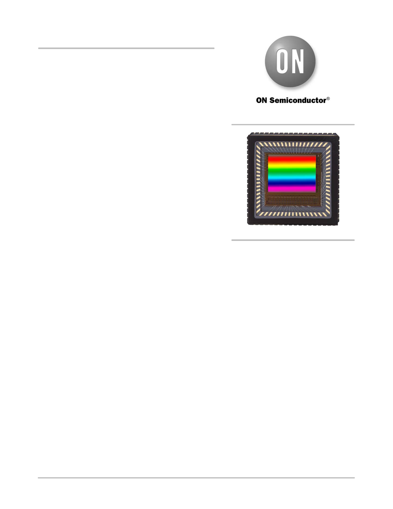
Figure 1. VITA 5000 Photo
Applications
• Machine Vision
• Motion Monitoring
• Security
• Barcode Scanning (2D)
Description
The VITA 5000 is a 1 inch Quad Super eXtended Graphics Array (QSXGA) CMOS image sensor with a pixel array of 2592
by 2048.
The high sensitivity 4.8 mm x 4.8 mm pixels support pipelined and triggered global shutter readout modes and can also be
operated in a low noise rolling shutter mode. In rolling shutter mode, the sensor supports correlated double sampling readout,
reducing noise and increasing the dynamic range.
The sensor has on-chip programmable gain amplifiers and 10-bit A/D converters. The integration time and gain parameters
can be reconfigured without any visible image artifact. Optionally the on-chip automatic exposure control loop (AEC) controls
these parameters dynamically. The image’s black level is either calibrated automatically or can be adjusted by adding a user
programmable offset.
A high level of programmability using a four wire serial peripheral interface enables the user to read out specific regions
of interest. Up to 8 regions can be programmed, achieving even higher frame rates.
The image data interface consists of eight LVDS lanes, facilitating frame rates up to 75 frames per second. Each channel runs
at 620 Mbps. A separate synchronization channel containing payload information is provided to facilitate the image
reconstruction at the receiver end.
The VITA 5000 is packaged in a 68-pin LCC package and is available in a monochrome and color version.
Contact your local ON Semiconductor office for more information.
© Semiconductor Components Industries, LLC, 2013
June, 2013 − Rev. 6
1
Publication Order Number:
NOIV1SN5000A/D
Free Datasheet http://www.datasheet4u.com/
1 page 
NOIV1SN5000A
Table 5. ELECTRICAL SPECIFICATIONS
Boldface limits apply for TJ = TMIN to TMAX, all other limits TJ = +30°C. (Notes 5, 6 and 7)
Parameter
Description
Min Typ Max Units
Power Supply Parameters
vdd_33
Supply voltage, 3.3 V
3.0 3.3 3.6
V
Idd_33
Current consumption 3.3 V supply
235 mA
vdd_18
Supply voltage, 1.8 V
1.6 1.8 2.0
V
Idd_18
Current consumption 1.8 V supply
115 mA
vdd_pix
Ptot
Supply voltage, pixel
Total power consumption at vdd_33 = 3.3 V, vdd_18 = 1.8 V
3.0 3.3 3.6
1000
V
mW
Pstby_lp
Power consumption in low power standby mode. (See Silicon Errata
on page 67)
50 mW
Popt
Power consumption at lower pixel rates
Configurable
I/O - LVDS (EIA/TIA-644): Conforming to standard/additional specifications and deviations listed
fserdata
Data rate on data channels
DDR signaling - 4 data channels, 1 synchronization channel;
620 Mbps
fserclock
Clock rate of output clock
Clock output for mesochronous signaling
310 MHz
Vicm
Tccsk
LVDS input common mode level
0.3 1.25 2.2
Channel to channel skew (Training pattern allows per channel skew
correction)
50
V
ps
Electrical/Interface
fin Input clock rate when PLL used
62 MHz
fin Input clock when LVDS input used
310 MHz
tidc Input clock duty cycle when PLL used
40 50 60
%
tj Input clock jitter
20 ps
fspi SPI clock rate when PLL used at fin = 62 MHz
10 MHz
Frame Specifications - Global Shutter
fps Frame rate at full resolution (global shutter)
75 fps
fps_roi1
fps_roi2
Xres x Yres = 2592 x 1944
Xres x Yres = 2048 x 2048
80 fps
92 fps
fps_roi3
Xres x Yres = 1024 x 1024
310 fps
fps_roi4
Xres x Yres = 640 x 480
860 fps
fps_roi5
Xres x Yres = 512 x 512
910 fps
fps_roi6
Xres x Yres = 256 x 256
2260
fps
FOT
Frame Overhead Time
45 ms
ROT
Row Overhead Time
1.1 ms
fpix Pixel rate (8 channels at 62 Mpix/s)
496 Mpix/s
5. All parameters are characterized for DC conditions after thermal equilibrium is established.
6. This device contains circuitry to protect the inputs against damage due to high static voltages or electric fields. However, it is recommended
that normal precautions be taken to avoid application of any voltages higher than the maximum rated voltages to this high impedance circuit.
7. Minimum and maximum limits are guaranteed through test and design.
For recommendations on power supply management guidelines, refer to application note AN65464: VITA 5000 HSMC
Cyclone Reference Board Design Recommendations.
http://onsemi.com
5
Free Datasheet http://www.datasheet4u.com/
5 Page 
NOIV1SN5000A
Rolling Shutter Mode
Another shutter mode supported by the sensor is the
rolling shutter mode. The shutter mechanism is an electronic
rolling shutter and the sensor operates in a streaming mode
similar to a video. This mechanism is controlled by the
on-chip sequencer logic. There are two Y pointers. One
points to the row that is to be reset for rolling shutter
operation, the other points to the row to be read out.
Functionally, a row is reset first and selected for read out
sometime later. The time elapsed between these two
operations is the exposure time.
Figure 9 schematically indicates the relative shift of the
integration times of different lines during the rolling shutter
operation. Each row is read and reset in a sequential way.
Each row in a particular frame is integrated for the same
time, but all lines in a frame ‘see’ a different stare time. As
a consequence, fast horizontal moving objects in the field of
view give rise to motion artifacts in the image; this is an
unavoidable property of a rolling shutter.
In rolling shutter mode, the pixel Fixed Pattern Noise
(FPN) is corrected on-chip by using the CDS technique.
After light integration on all pixels in a row is complete, the
storage node in the pixel is reset. Afterwards the integrated
signal is transferred to that pixel storage node. The
difference between the reset level and integrated signal is the
FPN corrected signal. The advantage of this technique,
compared to the DS technique used in the global shutter
modes, is that the reset noise of the pixel storage node is
cancelled. This results in a lower temporal noise level.
Figure 9. Rolling Shutter Operation
http://onsemi.com
11
Free Datasheet http://www.datasheet4u.com/
11 Page | ||
| Páginas | Total 30 Páginas | |
| PDF Descargar | [ Datasheet NOIV1SN5000A.PDF ] | |
Hoja de datos destacado
| Número de pieza | Descripción | Fabricantes |
| NOIV1SN5000A | VITA 5000 5.3 Megapixel 75 FPS Global Shutter CMOS Image Sensor | ON Semiconductor |
| Número de pieza | Descripción | Fabricantes |
| SLA6805M | High Voltage 3 phase Motor Driver IC. |
Sanken |
| SDC1742 | 12- and 14-Bit Hybrid Synchro / Resolver-to-Digital Converters. |
Analog Devices |
|
DataSheet.es es una pagina web que funciona como un repositorio de manuales o hoja de datos de muchos de los productos más populares, |
| DataSheet.es | 2020 | Privacy Policy | Contacto | Buscar |