|
|
|
PDF DMN3112SSS Data sheet ( Hoja de datos )
| Número de pieza | DMN3112SSS | |
| Descripción | SINGLE N-CHANNEL ENHANCEMENT MODE MOSFET | |
| Fabricantes | Diodes | |
| Logotipo | ||
Hay una vista previa y un enlace de descarga de DMN3112SSS (archivo pdf) en la parte inferior de esta página. Total 4 Páginas | ||
|
No Preview Available !
Features
• Low On-Resistance
• 57mΩ @ VGS = 10V
• 112mΩ @ VGS = 4.5V
• Low Gate Threshold Voltage
• Low Input Capacitance
• Fast Switching Speed
• Low Input/Output Leakage
• Lead Free By Design/RoHS Compliant (Note 2)
• "Green" Device (Note 4)
• Qualified to AEC-Q101 Standards for High Reliability
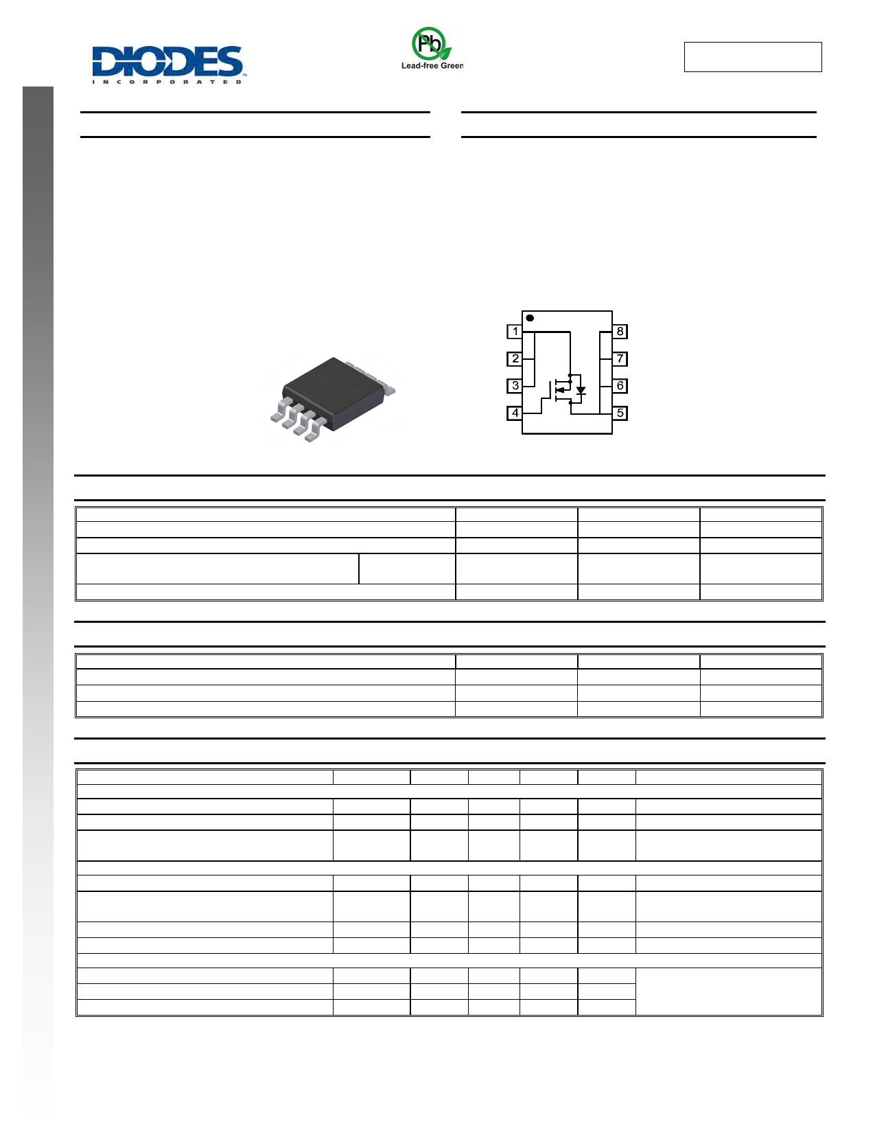
DMN3112SSS
SINGLE N-CHANNEL ENHANCEMENT MODE MOSFET
Please click here to visit our online spice models database.
Mechanical Data
• Case: SOP-8L
• Case Material: Molded Plastic, “Green” Molding Compound.
UL Flammability Classification Rating 94V-0
• Moisture Sensitivity: Level 1 per J-STD-020D
• Terminals Connections: See Diagram
• Terminals: Finish - Matte Tin annealed over Copper lead
frame. Solderable per MIL-STD-202, Method 208
• Marking Information: See Page 4
• Ordering Information: See Page 4
• Weight: 0.072g (approximate)
SOP-8L
S
D
SD
SD
GD
TOP VIEW
Maximum Ratings @TA = 25°C unless otherwise specified
Characteristic
Drain-Source Voltage
Gate-Source Voltage
Drain Current (Note 1)
Steady
State
Pulsed Drain Current (Note 3)
TA = 25°C
TA = 70°C
TOP VIEW
Internal Schematic
Symbol
VDSS
VGSS
ID
IDM
Value
30
±20
6
4.5
24
Units
V
V
A
A
Thermal Characteristics
Characteristic
Total Power Dissipation (Note 1)
Thermal Resistance, Junction to Ambient
Operating and Storage Temperature Range
Symbol
PD
RθJA
TJ, TSTG
Value
2.5
50
-55 to +150
Unit
W
°C/W
°C
Electrical Characteristics @TA = 25°C unless otherwise specified
Characteristic
OFF CHARACTERISTICS (Note 5)
Drain-Source Breakdown Voltage
Zero Gate Voltage Drain Current
Gate-Source Leakage
ON CHARACTERISTICS (Note 5)
Gate Threshold Voltage
Static Drain-Source On-Resistance
Forward Transconductance
Diode Forward Voltage (Note 5)
DYNAMIC CHARACTERISTICS
Input Capacitance
Output Capacitance
Reverse Transfer Capacitance
Symbol
BVDSS
IDSS
IGSS
VGS(th)
RDS(ON)
gfs
VSD
Ciss
Coss
Crss
Min Typ Max Unit
Test Condition
30 ⎯ ⎯
V VGS = 0V, ID = 250μA
⎯ ⎯ 800 nA VDS = 30V, VGS = 0V
⎯
⎯
⎯
⎯
±80
±800
nA VGS = ±20V, VDS = 0V
VGS = ±25V, VDS = 0V
1 ⎯ 2.2 V VDS = VGS, ID = 250μA
⎯
43
83
57
112
mΩ
VGS = 10V, ID = 5.8A
VGS = 4.5V, ID = 3.7A
⎯ 2.8 ⎯
S VDS = 10V, ID = 3.7A
0.5 0.8 1.2
V VGS = 0V, IS = 2.1A
⎯ 268 ⎯
⎯ 73 ⎯
⎯ 50 ⎯
pF
pF
VDS = 15V, VGS = 0V
f = 1.0MHz
pF
Notes:
1. Device mounted on 2 oz copper pad layout with RθJA = 50°C/W.
2. No purposefully added lead.
3. Pulse width ≤10μS, Duty Cycle ≤1%.
4. Diodes Inc.'s "Green" policy can be found on our website at http://www.diodes.com/products/lead_free/index.php.
5. Short duration pulse test used to minimize self-heating effect.
DMN3112SSS
Document number: DS31582 Rev. 1 - 2
1 of 4
www.diodes.com
October 2008
© Diodes Incorporated
Free Datasheet http://www.datasheet4u.com/
1 page | ||
| Páginas | Total 4 Páginas | |
| PDF Descargar | [ Datasheet DMN3112SSS.PDF ] | |
Hoja de datos destacado
| Número de pieza | Descripción | Fabricantes |
| DMN3112SSS | SINGLE N-CHANNEL ENHANCEMENT MODE MOSFET | Diodes |
| Número de pieza | Descripción | Fabricantes |
| SLA6805M | High Voltage 3 phase Motor Driver IC. |
Sanken |
| SDC1742 | 12- and 14-Bit Hybrid Synchro / Resolver-to-Digital Converters. |
Analog Devices |
|
DataSheet.es es una pagina web que funciona como un repositorio de manuales o hoja de datos de muchos de los productos más populares, |
| DataSheet.es | 2020 | Privacy Policy | Contacto | Buscar |