|
|
|
PDF FR9886 Data sheet ( Hoja de datos )
| Número de pieza | FR9886 | |
| Descripción | 380KHz Synchronous Step-Down DC/DC Converter | |
| Fabricantes | fitipower integrated technology | |
| Logotipo | ||
 1. 380KHz Synchronous Step-Down DC/DC Converter Hay una vista previa y un enlace de descarga de FR9886 (archivo pdf) en la parte inferior de esta página. Total 14 Páginas | ||
|
No Preview Available !
fitipower integrated technology lnc.
FR9886
23V, 2.5A, 340KHz Synchronous Step-Dow85nT
DC/DC Converter
Description
The FR9886 is a synchronous step-down DC/DC
converter that provides wide 4.5V to 23V input
voltage range and 2.5A continuous load current
capability.
The FR9886 fault protection includes cycle-by-cycle
current limit, input UVLO, output over voltage
protection and thermal shutdown. Besides,
adjustable soft-start function prevents inrush current
at turn-on. This device uses current mode control
scheme which provides fast transient response.
Internal Compensation function reduces external
compensation components and simplifies the design
process. In shutdown mode, the supply current is
less than 1uA.
The FR9886 is available in an 8-pin SOIC package,
provides a very compact system solution and good
thermal conductance.
Features
● High Efficiency Up to 96%
● Low Rds(on) integrated Power MOSFET
● Internal Compensation Function
● Wide Input Voltage Range: 4.5V to 23V
● Adjustable Output Voltage Range: 0.925V to
20V
● 2.5A Output Current
● Fixed 340KHz Switching Frequency
● Current Mode Operation
● Adjustable Soft-Start
● Cycle-by-Cycle current limit
● Input Under Voltage Lockout
● Over-Temperature Protection With Auto
Recovery
● <1uA Shutdown Current
● SOP-8 and SOP-8 Exposed Pad Package
Applications
● Set-Top-Box (STB)
● Televisions
● Distributed Power Systems
● XDSL Modems
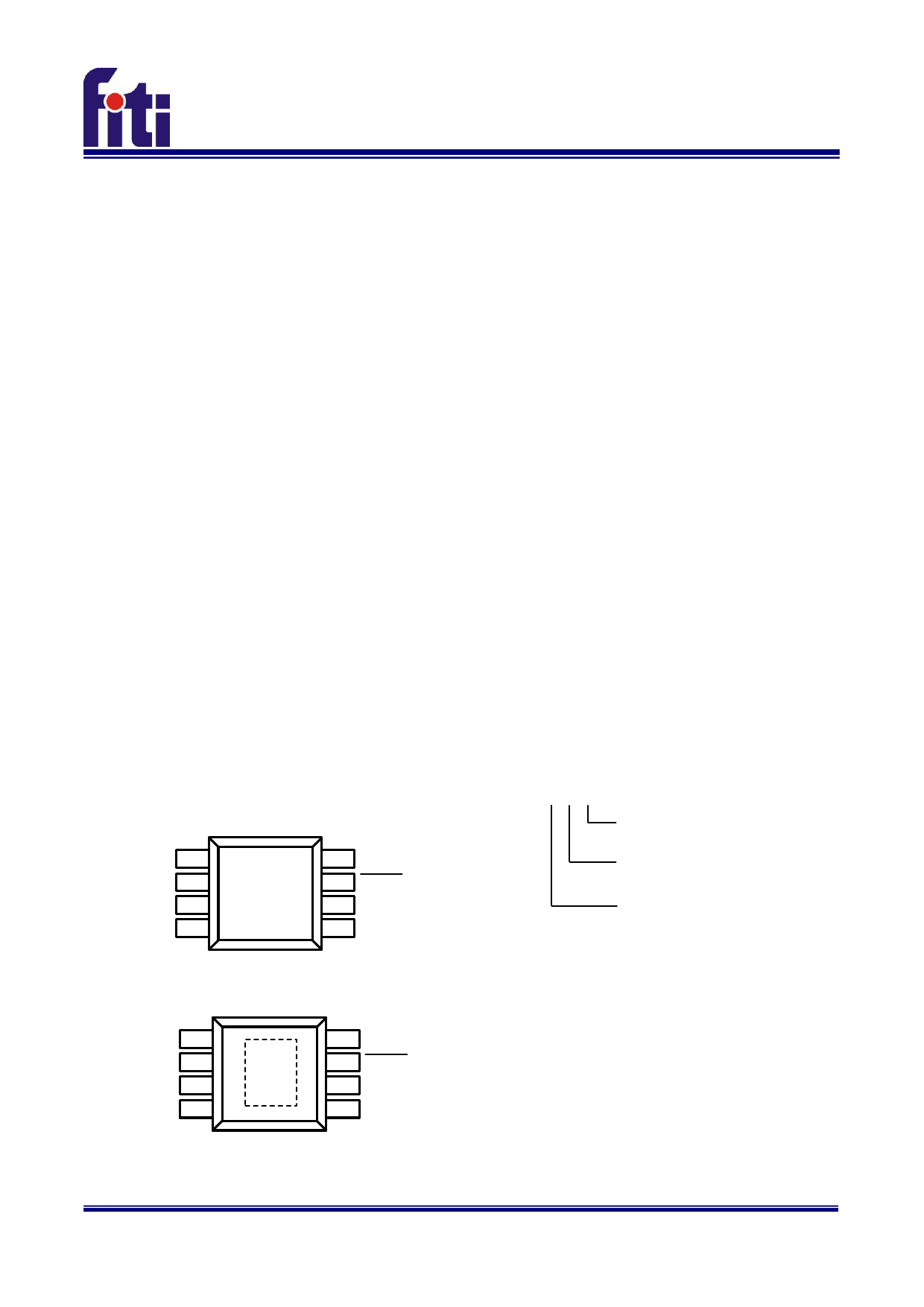
Pin Assignments
SO Package (SOP- 8)
BOOST
VIN
LX
GND
1
2
3
4
8
7
6
5
SS
SHDN
NC
FB
SP Package (SOP- 8 Exposed pad )
BOOST
VIN
LX
GND
1
2
3
4
8 SS
7 SHDN
6 NC
5 FB
Figure 1. Pin Assignment of FR9886
FR9886- 1.0-APR-2011
Ordering Information
FR9886□□□
TR: Tape / Reel
G: Green
Package Type
SO: SOP-8
SP: SOP-8(Exposed Pad)
1
Free Datasheet http://www.datasheet4u.com/
1 page 
fitipower integrated technology lnc.
Electrical Characteristics
(VIN=12V, TA=25 , unless otherwise specified.)
Parameter
Symbol
Conditions
VIN Input Supply Voltage
VIN Quiescent Current
VIN Shutdown Supply Current
Feedback Voltage
Feedback OVP Threshold Voltage
High-Side MOSFET RDS(ON) (Note3)
Low-Side MOSFET RDS(ON) (Note3)
High-Side MOSFET Leakage Current
High-Side MOSFET Current Limit (Note3)
Low-Side MOSFET Current Limit (Note3)
Error Amplifier Voltage Gain (Note3)
VIN
IDDQ
ISD
VFB
VOVP
RDS(ON)
RDS(ON)
ILX(leak)
ILIMIT(HS)
ILIMIT(LS)
VSHDN=1.8V, VFB=1.0V
VSHDN=0V
4.5V≦VIN≦23V
VSHDN=0V, VLX=0V
Minimum Duty
From Drain to Source
Oscillation frequency
FOSC
Short Circuit Oscillation Frequency
FOSC(short) VFB=0V
Maximum Duty Cycle
DMAX
VFB=0.8V
Minimum On Time (Note3)
TMIN
Input UVLO Threshold
Under Voltage Lockout
Hysteresis
VUVLO(Vth) VIN Rising
Threshold VUVLO(HYS)
Soft-Start Current
ISS VSS=0V
Soft-Start Period
TSS CSS=0.1uF
SHDN Input Low Voltage
VSHDN (L)
SHDN Input High Voltage
VSHDN (H)
SHDN Input Current
ISHDN
VSHDN=2V
Thermal Shutdown Threshold (Note3)
TSD
Note3:Not production tested.
FR9886
85T
Min Typ Max Unit
4.5
2.5
0.9 0.925
1.5
120
100
3.5 4.5
1.5
400
290 340
110
90
100
4.3
23
1
0.95
10
420
V
mA
μA
V
V
mΩ
mΩ
uA
A
A
V/V
KHz
KHz
%
ns
V
250 mV
6 uA
15 ms
0.4 V
2V
2 uA
170 ℃
FR9886- 1.0-APR-2011
5
Free Datasheet http://www.datasheet4u.com/
5 Page 
fitipower integrated technology lnc.
Application Information
FR9886
85T
VRIPPLE(ESR)=IL R(ESR)
VRIPPLE(ESL)=IL L(ESL) FOSC
1
D 1 D
VRIPPLE(C)=IL
1
8 COUT FOSC
IL
VOUT
FOSC L
1
VOUT
VIN
Where Δ IL is the peak-to-peak inductor ripple
current, FOSC is the switching frequency, L is the
inductance value, VIN is the input voltage, VOUT is the
output voltage, R(ESR) is the equivalent series
resistance value of the output capacitor, L(ESL) is the
equivalent series inductance value of the output
capacitor and the COUT is the output capacitor. The
following diagram is an example to graphical
represent Δ IL equation.
L=4.7uH
L=6.8uH
L=10uH
VOUT=3.3V, FOSC=340KHz
Low ESR capacitors are preferred. Ceramic,
tantalum or low ESR electrolytic capacitors can be
used depending on the output ripple requirement.
When using the ceramic capacitors, the ESL
component is usually negligible.
It is important to use the proper method to eliminate
high frequency noise when measuring the output
ripple. The figure shows how to locate the probe
across the capacitor when measuring output ripple.
Removing the scope probe plastic jacket in order to
expose the ground at the tip of the probe. It gives a
very short connection from the probe ground to the
capacitor and eliminating noise.
Probe Ground
VOUT
GND
Ceramic Capacitor
Output Inductor Selection
The output inductor is used for storing energy
and filtering output ripple current. But the
trade-off condition often happens between
maximum energy storage and the physical size
of the inductor. The first consideration for
selecting the output inductor is to make sure
that the inductance is large enough to keep the
converter in the continuous current mode.
That will lower ripple current and result in lower
output ripple voltage. The inductance value
should be determined to set the peak-to-peak
inductor ripple current Δ IL around 20% to 50%
of the maximum load current. Then the
inductance can be calculated with the following
equation:
IL= 0.2~0.5 IOUT(MAX)
L
VIN-VOUT
FOSC
VOUT
ΔIL
VIN
To guarantee sufficient output current, peak
inductor current must be lower than the FR9886
high-side MOSFET current limit. The peak
inductor current is as below:
IPEAK=IOUT(MAX)+ ΔIL
2
FR9886- 1.0-APR-2011
11
Free Datasheet http://www.datasheet4u.com/
11 Page | ||
| Páginas | Total 14 Páginas | |
| PDF Descargar | [ Datasheet FR9886.PDF ] | |
Hoja de datos destacado
| Número de pieza | Descripción | Fabricantes |
| FR9882 | 340KHz Synchronous Step-Down DC/DC Converter | Fiti |
| FR9884 | 340KHz Synchronous Step-Down DC/DC Converter | Fiti |
| FR9885 | Synchronous Step-Down DC/DC Converter | Fiti |
| FR9886 | 380KHz Synchronous Step-Down DC/DC Converter | fitipower integrated technology |
| Número de pieza | Descripción | Fabricantes |
| SLA6805M | High Voltage 3 phase Motor Driver IC. |
Sanken |
| SDC1742 | 12- and 14-Bit Hybrid Synchro / Resolver-to-Digital Converters. |
Analog Devices |
|
DataSheet.es es una pagina web que funciona como un repositorio de manuales o hoja de datos de muchos de los productos más populares, |
| DataSheet.es | 2020 | Privacy Policy | Contacto | Buscar |