|
|
|
PDF BM60013FV-C Data sheet ( Hoja de datos )
| Número de pieza | BM60013FV-C | |
| Descripción | 1ch Gate Driver Providing Galvanic Isolation | |
| Fabricantes | ROHM Semiconductor | |
| Logotipo | ||
Hay una vista previa y un enlace de descarga de BM60013FV-C (archivo pdf) en la parte inferior de esta página. Total 33 Páginas | ||
|
No Preview Available !
BM60013FV-C
Datasheet
Gate Driver Providing Galvanic isolation Series
Isolation voltage 2500Vrms
1ch Gate Driver Providing Galvanic Isolation
BM60013FV-C
●General Description
The BM60013FV-C is a gate driver with isolation voltage
2500Vrms, I/O delay time of 200ns, and minimum input
pulse width of 100ns, and incorporates the fault signal
output functions, undervoltage lockout (UVLO) function,
thermal protection function, and short current protection
(SCP, DESAT) function.
●Features
■ Providing Galvanic Isolation
■ Active Miller Clamping
■ Fault signal output function
(Adjustable output holding time)
■ Undervoltage lockout function
■ Thermal protection function
(Adjustable threshold voltage)
■ Short current protection function
(Adjustable threshold voltage)
■ Soft turn-off function for short current protection
●Key Specifications
■ Isolation voltage:
■ Maximum gate drive voltage:
■ I/O delay time:
■ Minimum input pulse width:
2500 [Vrms] (Min.)
20 [V] (Max.)
200 [ns] (Max.)
100 [ns] (Max.)
●Package
SSOP-B20W
W(Typ.) x D(Typ.) x H(Max.)
6.50 ㎜×8.10 ㎜×2.01 ㎜
●Applications
■ Automotive isolated IGBT/MOSFET inverter gate drive
■ Automotive DC-DC converter
■ Industrial inverters systems
■ UPS systems
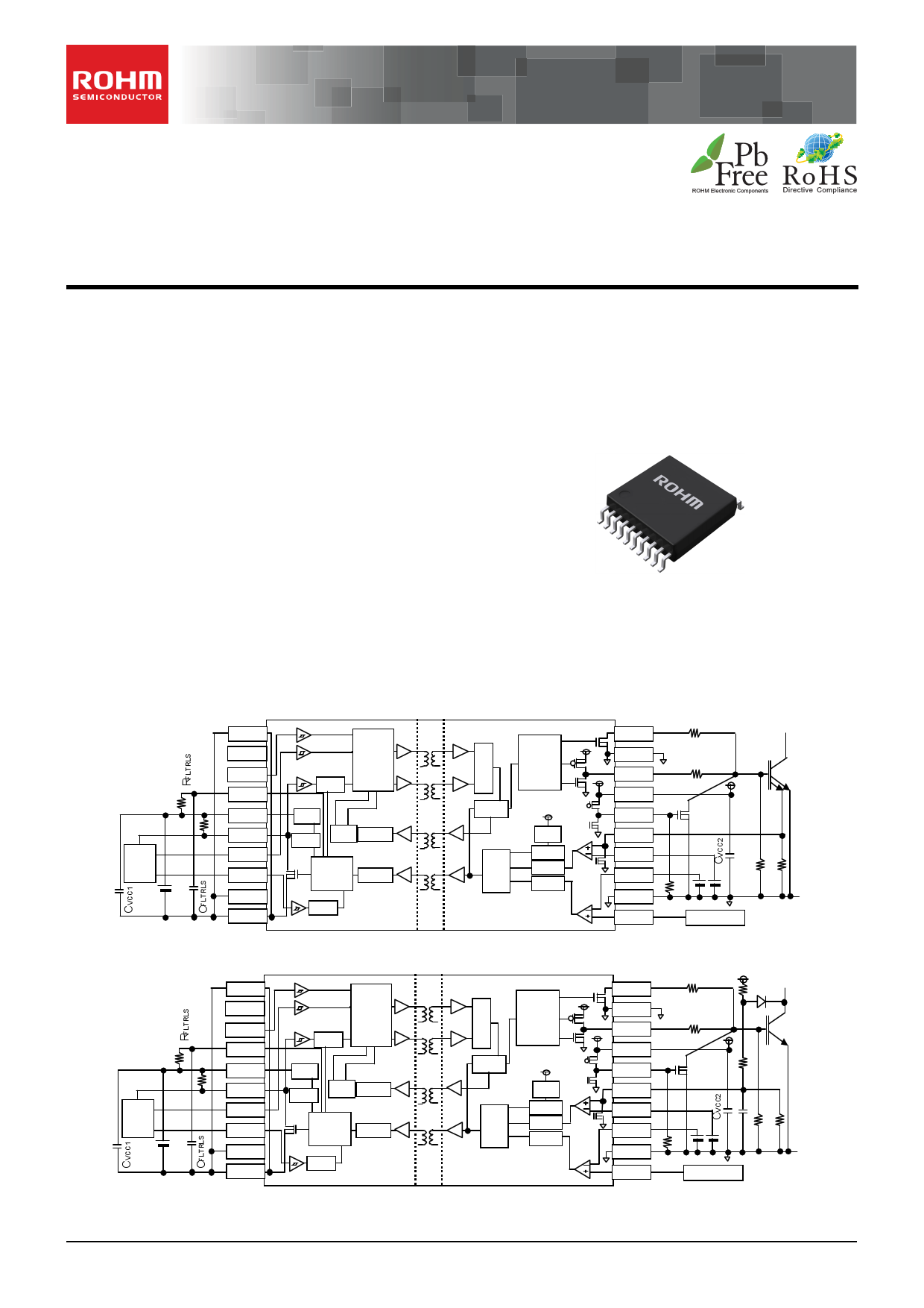
● Typical Application Circuits
ECU
GND1
NC
INB
FLTRLS
VCC1
FLT
INA
ENA
TEST
GND1
MASK
LOGIC
UVLO
MASK
FB TIMER
FLT TIMER
MASK
S
Q
R
LOGIC
FLT
PRE
DRIVER
UVLO
MASK
MASK
MASK
PROOUT
GND2
OUT1
VCC2
OUT2
SCPIN
SCPTH
VTSTH
GND2
VTSIN
Figure 1. For using 4-pin IGBT (for using SCP function)
Sens or
ECU
GND1
NC
INB
FLTRLS
VCC1
FLT
INA
ENA
TEST
GND1
MASK
LOGIC
UVLO
MASK
FB TIMER
FLT TIMER
MASK
S
Q
R
LOGIC
FLT
PRE
DRIVER
UVLO
MASK
MASK
MASK
PROOUT
GND2
OUT1
VCC2
OUT2
SCPIN
SCPTH
VTSTH
GND2
VTSIN
Figure 2. For using 3-pin IGBT (for using DESAT function)
Sens or
○Product structure:Silicon monolithic integrated circuit
.www.rohm.com
© 2012 ROHM Co., Ltd. All rights reserved.
TSZ22111・14・001
○This product is not designed protection against radioactive rays
1/30
TSZ02201-0717ABH00020-1-2
29.May.2012 Rev.002
Free Datasheet http://www.datasheet4u.com/
1 page 
BM60013FV-C
Datasheet
2) Fault status output
This function is used to output a fault signal from the FLT pin when an fault occurs (i.e., when the undervoltage lockout
function (UVLO), short current protection function (SCP) or thermal protection function is activated) and hold the fault
signal until the set Fault output holding time is completed. The fault output holding time tFLTRLS is given as the following
equation with the settings of capacitor CFLTRLS and resistor RFLTRLS connected to the FLTRLS pin. For example, when
CFLTRLS is set to 0.01F and RFLTRLS is set to 200k, the holding time will be set to 2 ms.
tFLTRLS [ms]= CFLTRLS [F]•RFLTRLS [k]
To set the fault output holding time to “0” ms, only connect the resistor RFLTRLS.
Status
Normal
Fault occurs
FLT pin
Hi-Z
L
Status
FLTRLS
Fault occurs (The UVLO, SCP or
thermal protection function is activated.)
VFLTRLS
ENA
UVLO
SCP
VTS
VCC1
MASK
MASK
MASK
MASK
FLT
SS
RR
Hi-Z
FLT
L
FLTRLS
+-
OUT1
H
L
Fault output holding time
(tFLTRLS)
Figure 6. Fault Status Output Timing Chart
ECU
FLT MASK
GND1
LOGIC
Figure 7. Fault Output Block Diagram
3) Undervoltage Lockout (UVLO) function
The BM60013FV-C incorporates the undervoltage lockout (UVLO) function both on the low and the high voltage sides.
When the power supply voltage drops to the UVLO ON voltage, the OUT1 pin and the FLT pin both will output the “L”
signal. When the power supply voltage rises to the UVLO OFF voltage, these pins will be reset. However, during the fault
output holding time set in “2) Fault status output” section, the OUT1 pin and the FLT pin will hold the “L” signal. In
addition, to prevent malfunctions due to noises, mask time tUVLO1MSK and tUVLO2MSK are set on both low and high
voltage sides.
IN
H
L
VCC1
FLT
OUT1
Figure 8. Input-side UVLO Function Operation Timing Chart
VUVLO1H
VUVLO1L
Hi-Z
L
H
L
IN
H
L
VCC2
FLT
OUT1
Figure 9. Output-side UVLO Operation Timing Chart
VUVLO2H
VUVLO2L
Hi-Z
L
HHL i-Z
www.rohm.com
© 2012 ROHM Co., Ltd. All rights reserved.
TSZ22111・15・001
5/30
TSZ02201-0717ABH00020-1-2
29.May.2012 Rev.002
5 Page 
BM60013FV-C
●Absolute maximum ratings
Parameter
Symbol
Limits
Input-side supply voltage
Output-side supply voltage
INA, INB, ENA pin input voltage
FLT pin input voltage
FLTRLS pin input voltage
VTSIN pin input voltage
SCPIN pin input voltage
VTSTH pin input voltage
SCPTH pin input voltage
OUT1 pin output current (DC)
VCC1
VCC2
VIN
VFLT
VFLTRLS
VVTSIN
VSCPIN
VVTSTH
VSCPTH
IOUT1
-0.3 to +7.0*1
-0.3 to +25.0*2
-0.3 to +VCC1+0.3 or +7.0*1
-0.3 to +VCC1+0.3 or +7.0*1
-0.3 to +VCC1+0.3 or +7.0*1
-0.3 to +7.0*2
-0.3 to +VCC2+0.3V or +25.0*2
-0.3 to +7.0*2
-0.3 to +VCC2+0.3V or +25.0*2
0.4*3
OUT1 pin output current (Peak 1us)
OUT2 pin output current (DC)
IOUT1PEAK
IOUT2
5.0
0.1*3
OUT2 pin output current (Peak 1us)
PROOUT pin output current
IOUT2PEAK
IPROOUT
1.0
0.2*3
FLT output current
Power dissipation
IFLT 10
Pd 1.19*4
Operating temperature range
Topr
-40 to +125
Storage temperature range
Tstg -55 to +150
Junction temperature
Tjmax
+150
*1 Relative to GND1.
*2 Relative to GND2.
*3 Should not exceed Pd and Tj=150C.
*4 Derate above Ta=25C at a rate of 9.5mW/C. Mounted on a glass epoxy of 70 mm 70 mm 1.6 mm.
Datasheet
Unit
V
V
V
V
V
V
V
V
V
A
A
A
A
A
mA
W
℃
℃
℃
●Recommended operating conditions
Parameter
Input-side supply voltage
Output-side positive supply voltage
Short current detection common mode input voltage
Thermal detection common mode input voltage
*5 Relative to GND1.
*6 Relative to GND2.
Symbol
VCC1*5
VCC2*6
VSCCM
VTSCM
Min.
4.5
14.0
0.0
0.0
Max.
5.5
20.0
2.5
3.0
Units
V
V
V
V
●Insulation related characteristics
Parameter
Insulation Resistance (VIO=500V)
Insulation Withstand Voltage / 1min
Insulation Test Voltage / 1sec
Symbol
RS
VISO
VISO
Characteristic
>109
2500
3000
Units
Ω
Vrms
Vrms
www.rohm.com
© 2012 ROHM Co., Ltd. All rights reserved.
TSZ22111・15・001
11/30
TSZ02201-0717ABH00020-1-2
29.May.2012 Rev.002
11 Page | ||
| Páginas | Total 33 Páginas | |
| PDF Descargar | [ Datasheet BM60013FV-C.PDF ] | |
Hoja de datos destacado
| Número de pieza | Descripción | Fabricantes |
| BM60013FV-C | 1ch Gate Driver Providing Galvanic Isolation | ROHM Semiconductor |
| Número de pieza | Descripción | Fabricantes |
| SLA6805M | High Voltage 3 phase Motor Driver IC. |
Sanken |
| SDC1742 | 12- and 14-Bit Hybrid Synchro / Resolver-to-Digital Converters. |
Analog Devices |
|
DataSheet.es es una pagina web que funciona como un repositorio de manuales o hoja de datos de muchos de los productos más populares, |
| DataSheet.es | 2020 | Privacy Policy | Contacto | Buscar |