|
|
PDF DS2710 Data sheet ( Hoja de datos )
| Número de pieza | DS2710 | |
| Descripción | Single-Cell NiMH Charger | |
| Fabricantes | Maxim Integrated | |
| Logotipo |  |
|
Hay una vista previa y un enlace de descarga de DS2710 (archivo pdf) en la parte inferior de esta página. Total 12 Páginas | ||
|
No Preview Available !
Rev 0; 4/08
Single-Cell NiMH Charger
General Description
The DS2710 is ideal for in-system charging of single-cell
nickel metal hydride (NiMH) cells for low-current
portable applications. Inputs to the DS2710 include USB
voltage sources and 5V regulated adapters.
Temperature, voltage, and charge time are monitored to
provide proper fast-charging control algorithms for
single-cell NiMH or nickel cadmium (NiCd) batteries.
The DS2710 includes battery tests to detect defective or
inappropriate cells such as alkaline primary batteries.
Applications
Small Rechargeable Devices
Voice Recorders
Cordless Mouse
Battery-Powered Toys
Typical Operating Circuit
CHARGE
SOURCE
GROUND
CS
VDD VP1
DS2710
THM
VN0 VN1
SENSE
NiMH
CELL
Features
♦ Charges Single-Cell NiMH Cells
♦ Switch-Mode Topologies Supported by Hysteretic
Control Technique
♦ Precharges Deeply Depleted Cells
♦ Fast-Charges NiMH with -ΔV Termination
Sensitivity of 2mV (typ)
♦ Monitors Voltage, Temperature, and Time for
Safety and Secondary Termination
♦ Regulates Charge Current
♦ Designed for External pMOS
♦ Rail-to-Rail MOSFET Driver
♦ Tiny 10-Pin TDFN Package (3mm x 4mm)
Ordering Information
PART
PIN-PACKAGE
DS2710G+
10 TDFN-EP*
DS2710G+T&R
10 TDFN-EP*
+Denotes a lead(Pb)-free/RoHS-compliant package.
T&R = Tape and reel.
*EP = Exposed pad.
Pin Configuration
TOP VIEW
VSS 1 +
CS 2
VDD 3
THM 4
STATUS 5
*EP
DS2710
10 VP1
9 VN1
8 VN0
7 TMR
6 CTEST
*EXPOSED PAD.
TDFN
(3mm × 4mm)
________________________________________________________________ Maxim Integrated Products 1
For pricing, delivery, and ordering information, please contact Maxim Direct at 1-888-629-4642,
or visit Maxim’s website at www.maxim-ic.com.
Free Datasheet http://www.datasheet4u.com/
1 page 
Single-Cell NiMH Charger
Detailed Description
Charge Algorithm Overview
The DS2710 controls switch-mode topology charging of
a single NiMH cell from a voltage-regulated charge
source. The IC is reset in one of two ways: with the
application of power to the DS2710 or after exiting
SUSPEND state. Once one of these conditions occurs,
the DS2710 enters the PRESENCE state and waits for a
cell to be inserted before starting a charge cycle.
Once a cell is detected, the DS2710 enters PRECHARGE
state and begins qualification to prevent fast charging
of deeply depleted cells or charging under extreme
temperature conditions. Precharging is performed at a
reduced rate until the cell reaches 1V. The algorithm
then proceeds to the FAST-CHARGE state, which
includes cell tests to avoid accidental charging of alka-
line cells or NiMH cells that are worn out or damaged.
Fast charging continues as long as all the cell qualifica-
tion criteria are met. Fast charging terminates by the
-ΔV (negative delta voltage) method. The TOP-OFF
charge phase follows to completely charge the cell.
After the TOP-OFF charge timer expires, the DS2710
enters the MAINTENANCE state to indefinitely keep the
cell at a full state of charge. Maximum voltage, temper-
ature, and charge-time monitoring during all charge
phases act as secondary or safety termination methods
to provide additional protection from overcharge. Any
error condition occurring during charge forces the
DS2710 into the FAULT state and charging terminates.
Charging can be halted at any time by floating the TMR
pin, which forces the DS2710 into SUSPEND state.
Once a charge is complete either normally or by
FAULT, the DS2710 remains in the final state (MAINTE-
NANCE or FAULT) until the cell is removed, the IC is
power cycled, or the IC is forced into SUSPEND state.
Afterwards, the DS2710 returns to PRESENCE state
and the charge cycle begins again.
An internal oscillator provides the main clock source
used to generate timing signals for chip operation. The
PRECHARGE timer, hold-off timers, and timing for CS
operation and cell testing are derived from this time
base. If the internal clock should ever fail, a watchdog-
detection circuit halts charging. The watchdog-safety
circuit and charge timer set by the TMR pin are derived
from oscillators other than the main clock source. Figure
1 is the DS2710 block diagram and Figure 2 is the state
diagram.
POWER-ON RESET (POR)
The UVLO circuit serves as a power-up and brownout
detector by monitoring VDD to prevent charging until
VDD rises above VUVLO, or when VDD drops below
VUVLO - VUHYS. If undervoltage lockout is active,
charging is prevented, the state machine is forced to
the POR state, and all charge timers are reset.
PRESENCE
The DS2710 enters the PRESENCE state whenever the
TMR pin is not floating and VDD > VUVLO, indicating
that the charge source is present. The DS2710 remains
in the PRESENCE state until a cell is inserted into the
circuit, causing the voltage of VP1 - VN1 to fall below
1.65V (VMAX-OPEN) and the cell temperature is inside a
valid charging range between 0°C and +45°C
(TTHM-MIN and TTHM-MAX when used with recommend-
ed thermistor and resistor values). If both these condi-
tions are met, the DS2710 enters PRECHARGE. If a cell
is inserted but the temperature is outside the valid
charging range, the DS2710 remains in the PRESENCE
state until the cell temperature falls within the valid
charging range.
PRECHARGE
The DS2710 enters the PRECHARGE state when a valid
cell voltage is detected and the cell temperature as
measured by the DS2710 thermistor circuit is within the
valid charging range. The DS2710 precharges the cell
by regulating the voltage drop across the sense resis-
tor to 113mV with a 25% duty cycle. The STATUS out-
put toggles at 1Hz to indicate the cell is being
precharged. Precharging lasts until the measured cell
voltage exceeds 1.0V (VLOW), at which time the
DS2710 enters the FAST-CHARGE state. If the cell volt-
age does not exceed VLOW within 30min (tPCHG) or if
the cell temperature exceeds +50°C (TTHM-STOP) at
any time during PRECHARGE, the DS2710 enters the
FAULT state. If at any time during PRECHARGE the cell
voltage exceeds 1.75V (VMAX-CHARGE), the DS2710
determines that the cell has been removed and enters
the FAULT state.
FAST-CHARGE
In the FAST-CHARGE state, the DS2710 regulates the
average voltage across the sense resistor to 113mV.
The STATUS output is held high to indicate the cell
pack is being charged. During FAST-CHARGE, the
DS2710 performs a cell test every 31s. The CELL TEST
state is responsible for determining when charge is
complete. As secondary overcharge protection, the
DS2710 terminates FAST-CHARGE and enters TOP-
OFF based on a time delay set by the external resistor
on the TMR pin. This resistor value can set the sec-
ondary charge termination delay to anywhere from
30min up to 5hr. If the cell temperature exceeds +50°C
at any time during FAST-CHARGE, the DS2710 enters
_______________________________________________________________________________________ 5
5 Page 
Single-Cell NiMH Charger
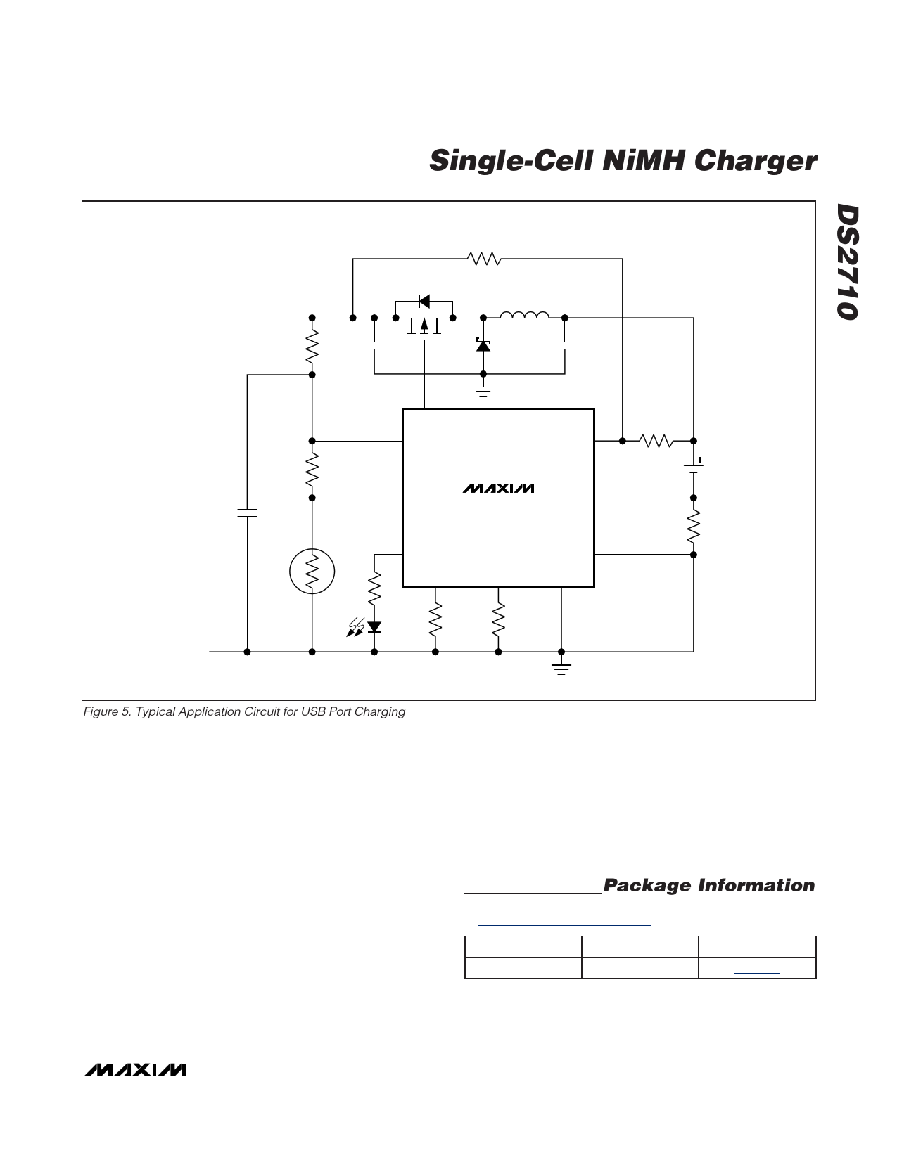
+5V
(USB+)
R1
150Ω
C2
10μF
CERAMIC
R3
270kΩ
Q1
ZXM62P02E6
L1
15μH
SISCDRH74M-150R
D2
1W B340A-13
SCHOTTKY
C3
10μF
CERAMIC
R4
10kΩ
C1
1μF
RT1
103AT-2
GROUND
(USB-)
CS
VDD
VP1
THM DS2710 VN1
STATUS
R2 TMR CTEST
1kΩ
D1
GREEN
SMA
R7
100kΩ
R8
47kΩ
VN0
VSS
R6
1kΩ
1S
NiMH
CELL
R9
0.1Ω
1W
Figure 5. Typical Application Circuit for USB Port Charging
Referring to the example circuit and layout of Figure 6,
the loop labeled as Loop1 encompassing CIN,
QSWITCH, and DSWITCH should be kept as small as
possible to minimize the change in loop area that
occurs when switching from the OFF to the ON state
and vice versa. Loop2 should also be minimized as
much as practical, although it contains DC current
components for the most part. The returning ground
currents should be allowed to follow a path on a layer
directly under the outgoing path since the high-fre-
quency components try to follow the path of least
impedance. Low ESR and ESL capacitors should be
used when possible and for all capacitors 10µF and
smaller. Typical surface-mount ceramic types with an
X5R or better dielectric are recommended.
Another important layout detail is the connection of the
sense resistor. Proper Kelvin connection layout should
be used to ensure the signal quality viewed by the
sensing circuit inside the DS2710 is adequate. Figure 7
shows a recommended connection of the sense lines to
the resistor footprint.
Package Information
For the latest package outline information and land patterns, go
to www.maxim-ic.com/packages.
PACKAGE TYPE PACKAGE CODE DOCUMENT NO.
10 TDFN-EP
T1034+1
21-0268
______________________________________________________________________________________ 11
11 Page | ||
| Páginas | Total 12 Páginas | |
| PDF Descargar | [ Datasheet DS2710.PDF ] | |
Hoja de datos destacado
| Número de pieza | Descripción | Fabricantes |
| DS2710 | Single-Cell NiMH Charger | Maxim Integrated |
| DS2711 | (DS2711 / DS2712) Loose Cell NiMH Chargers | Maxim Integrated Products |
| DS2712 | (DS2711 / DS2712) Loose Cell NiMH Chargers | Maxim Integrated Products |
| DS2714 | Quad Loose Cell NiMH Charger | Maxim Integrated Products |
| Número de pieza | Descripción | Fabricantes |
| SLA6805M | High Voltage 3 phase Motor Driver IC. |
Sanken |
| SDC1742 | 12- and 14-Bit Hybrid Synchro / Resolver-to-Digital Converters. |
Analog Devices |
|
DataSheet.es es una pagina web que funciona como un repositorio de manuales o hoja de datos de muchos de los productos más populares, |
| DataSheet.es | 2020 | Privacy Policy | Contacto | Buscar |
