|
|
|
PDF IR1152S Data sheet ( Hoja de datos )
| Número de pieza | IR1152S | |
| Descripción | uPFC ONE CYCLE CONTROL PFC IC | |
| Fabricantes | International Rectifier | |
| Logotipo | ||
Hay una vista previa y un enlace de descarga de IR1152S (archivo pdf) en la parte inferior de esta página. Total 20 Páginas | ||
|
No Preview Available !
Feb 21, 2011
IR1152S
FIXED 66kHz FREQUENCY, µPFC ONE CYCLE CONTROL PFC
IC WITH BROWN-OUT PROTECTION
Features
• PFC IC with IR proprietary “One Cycle Control”
• Continuous conduction mode boost type PFC
• Fixed 66kHz switching frequency
• Average current mode control
• Input line sensed brownout protection
• Output overvoltage protection
• Open loop protection
• Cycle by cycle peak current limit
• VCC under voltage lockout
• Programmable soft start
• Micropower startup
• User initiated micropower “Sleep Mode”
• 750mA peak gate drive
• Latch immunity and ESD protection
Description
µPFC IR1152 power factor correction IC, based on IR proprietary "One
Cycle Control" (OCC) technique, provides for high PF and excellent DC
Bus regulation while enabling drastic reduction in component count,
PCB area and design time as compared to traditional solutions. The IC
is designed to operate in 85-264VAC universal input, continuous
conduction mode Boost PFC at fixed 66kHz switching frequency.
IR1152 features include input-line sensed brown-out protection,
overvoltage protection, cycle by cycle peak current limit, open loop
protection, VCC UVLO, soft-start and micropower startup current of less
than 75µA. In addition, for standby power requirements, the IC can be
http://www.DataSheet4U.com/
driven into a micropower sleep mode by pulling the OVP/EN pin low
where the current consumption is less than 75uA. The IR1152 is
available in SO-8 packages.
Package
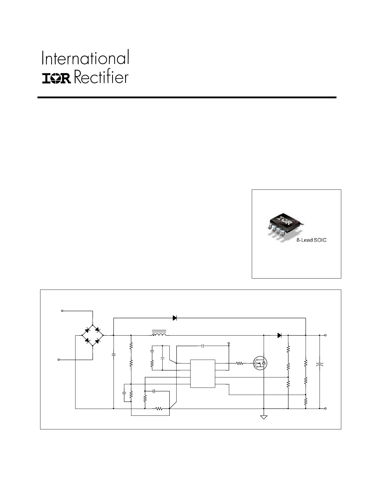
IR1152 Application Diagram
ACIN1
-+
ACIN2
VCC
1 COM GATE 8
2 COMP VCC 7
3 ISNS
VFB 6
4 BOP OVP/EN 5
IR1152
VOUT
+
RTN
www.irf.com
© 2011 International Rectifier
1 page 
IR1152S
Current Amplifier Section
Parameters
DC Gain
Corner Frequency
Input Offset Voltage
ISNS Input Bias Current
Blanking Time
Symbol
gDC
fC
VIO
IISNS(Bias)
TBLANK
Min.
2.65
-57
170
Typ.
3.1
5
4
320
Max.
3.55
16
-13
470
Units
V/V
kHz
mV
µA
ns
Remarks
Average Current Mode, Note 1
Note 1
VFB=0V, VISNS=-1V
Gate Driver Section
Parameters
Symbol Min. Typ. Max.
Gate Low Voltage
Gate High Voltage
VGLO
0.8
VGTH
12
10
13
14
Rise Time
tr
25
60
Fall Time
tf
35
65
Output Peak Current
IOPK 750
Gate Voltage at Fault
VG fault
0.08
Note 1: Guaranteed by design, but not tested in production
Units
V
V
ns
ns
ns
ns
mA
V
Remarks
IGATE = 200mA
VCC=17V, Internally Clamped
VCC=11.5V
CLOAD = 1nF, VCC=15V
CLOAD = 4.7nF, VCC=15V
CLOAD = 1nF, VCC=15V
CLOAD = 4.7nF, VCC=15V
CLOAD = 4.7nF, VCC=15V, Note 1
IGATE = 20mA
http://www.DataSheet4U.com/
www.irf.com
5 © 2011 International Rectifier
5 Page 
IR1152S
IR1152 Modes of operation
Referenced to States & Transition Diagram
UVLO/Sleep Mode: The IC is in the UVLO/Sleep
mode when VCC pin voltage is below VCC,ON at
start-up or when VCC pin voltage drops below
VCC,UVLO during normal operation or when OVP/EN
pin voltage is below VSLEEP. The UVLO/Sleep
mode is accessible from any other state of
operation. This mode can be actively invoked by
pulling the OVP/EN pin below VSLEEP even if VCC
pin voltage is above VCC,ON. In the UVLO/Sleep
state, the gate drive circuit is inactive, most of the
internal circuitry is unbiased and the IC draws a
quiescent current of ISLEEP which is less than
75uA. Also, the internal logic of the IC ensures
that whenever the Sleep mode is actively invoked,
the COMP pin is actively discharged below
VCOMP,START threshold prior to entering the sleep
mode, in order to facilitate soft-start upon
resumption of operation.
Stand-by Mode: The IC is placed in Stand-by
mode whenever an Open-loop and/or a Brown-out
situation is detected. A Brown-out situation is
sensed when BOP pin voltage is less than
VBOP(EN) prior to system start-up and when BOP
pin voltage drops below VBOP after start-up. An
Open-loop situation is sensed anytime VFB pin
voltage is less than VOLP. All internal circuitry is
biased in the Stand-by Mode, but the gate is
inactive and the IC draws a few mA of current.
This state is accessible from any other state of
operation of the IC. COMP pin is actively
discharged to below VCOMP,START whenever this
state is entered from normal operation in order to
facilitate soft-start upon resumption of operation.
Soft Start Mode: During system start-up, the soft-
start mode is activated once the VCC voltage has
exceeded VCC,ON, the VFB pin voltage has
exceeded VOLP and BOP pin voltage has
exceeded VBOP(EN) and VCOMP voltage is less
than VCOMP,START i.e. a pre-bias on COMP pin
greater than VCOMP,START threshold will not allow IC
to commence operation. The soft start time is the
time required for the VCOMP voltage to charge
through its entire dynamic range i.e. through
VCOMP,EFF. As a result, the soft-start time is
dependent upon the component values selected
for compensation of the voltage loop on the
COMP pin. To an extent, keeping in mind the
voltage feedback loop considerations, the soft-
system start time is programmable.
As VCOMP voltage rises gradually, the IC allows
a higher and higher RMS current into the PFC
converter. This controlled increase of the input
current amplitude contributes to reducing system
component stress during start-up.
Normal Mode: The IC enters the normal
operating mode once the soft start transition has
been completed (for all practical purposes there is
essentially no difference between the soft-start
and normal modes). At this point the gate drive is
switching and all protection functions of the IC are
active. If, from the normal mode, the IC is pushed
into either a Stand-by mode or UVLO/Sleep mode
then COMP pin is actively discharged below
VCOMP,START and system will go through soft-start
upon resumption of operation.
OVP Mode: The IC enters OVP mode whenever
an overvoltage condition is detected. A system
overvoltage condition is recognized when VFB
and/or OVP/EN pin voltage exceeds VOVP
threshold. When this happens the IC immediately
disables the gate drive and holds it in that state.
The gate drive is re-enabled only when both
OVP/EN and VFB pin voltages are less than
VOVP(RST) threshold. This state is accessible from
both the soft start and normal modes of operation.http://www.DataSheet4U.com/
IPK LIMIT Mode: The IC enters IPK LIMIT mode
whenever the magnitude of ISNS pin voltage
exceeds the VISNS(PK) threshold triggering cycle-by-
cycle peak over-current protection. When this
happens, the IC immediately disables the gate
drive and holds it in that state. Gate drive is re-
enabled when magnitude of ISNS pin voltage
drops below VISNS(PK) threshold. This state is
accessible from both the soft start and normal
modes of operation.
www.irf.com
11 © 2011 International Rectifier
11 Page | ||
| Páginas | Total 20 Páginas | |
| PDF Descargar | [ Datasheet IR1152S.PDF ] | |
Hoja de datos destacado
| Número de pieza | Descripción | Fabricantes |
| IR1152S | uPFC ONE CYCLE CONTROL PFC IC | International Rectifier |
| Número de pieza | Descripción | Fabricantes |
| SLA6805M | High Voltage 3 phase Motor Driver IC. |
Sanken |
| SDC1742 | 12- and 14-Bit Hybrid Synchro / Resolver-to-Digital Converters. |
Analog Devices |
|
DataSheet.es es una pagina web que funciona como un repositorio de manuales o hoja de datos de muchos de los productos más populares, |
| DataSheet.es | 2020 | Privacy Policy | Contacto | Buscar |