No Preview Available !

AP8012
Chipown
GREEN POWER
OFF LINE SMPS PRIMARY SWITCHE
Features
z 85v to 265v wide range AC voltage input
z A 730v MOSFET on the same silicon chip
z Auto start up with high voltage current source
z PWM with current mode control
z 10v to 39v wide range VCC voltage
z Fixed 55KHz switching frequency
z Automatic skip cycle mode in low load condition.
z Over temperature, over current and over voltage
protection
z Auxiliary under voltage lockout with hysteresis
z Electromagnetic Oven power supplies
z Air Conditioner power supplies
z AC/DC LED Driver Applications
Package
Type
European (195-265 Vac)
US (85-265 Vac)
SO8 DIP8
8W 13W
5 W 8W
Applications
z Power AC/DC Adapters for Chargers
Typical Application
AC
+
DC
-
COMP
VCC SW
AP8012
GND
4/F, Building F, IT industry Park No.21 Changjiang Road, Wuxi New Destrict Tel: +86(510)8521-7718 Ver 2.0 http://www.chipown.com.cn
-1-

AP8012
Chipown
Functional Description
1. Startup
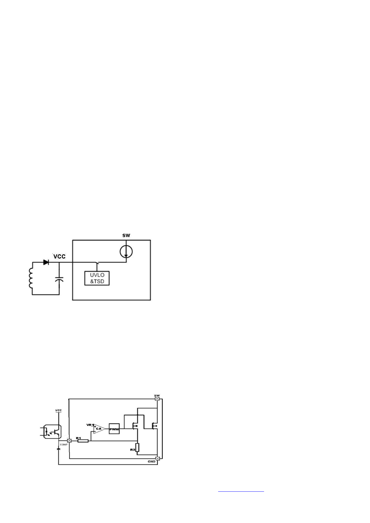
This device includes a high voltage start up current source
connected on the SW of the device. As soon as a voltage is
applied on the input of the converter, this start up current
source is activated and to charge the VCC capacitor as
long as VCC is lower than VSTART. When reaching
VSTART, the start up current source is cut off by
UVLO&TSD and the device begins to operate by turning
on and off its main power MOSFET. As the COMP pin
does not receive any current from the opto-coupler, the
device operates at full current capacity and the output
voltage rises until reaching the regulation point where the
secondary loop begins to send a current in the opto-coupler.
At this point, the converter enters a regulated operation
where the COMP pin receives the amount of current
needed to deliver the right power on secondary side.
Fig 1 Startup circuit
2. Feedback
A feedback pin controls the operation of the device. Unlike
conventional PWM control circuits which use a voltage
input, the COMP pin is sensitive to current. Figure 2
presents the internal current mode structure. The Power
MOSFET delivers a sense current which is proportional to
the main current. R2 receives this current and the current
coming from the COMP pin. The voltage across R2 VR2 is
Fig 2 Feedback Circuit
then compared to a fixed reference voltage. The MOSFET
is switched off when VR2 equals the reference voltage.
3. Leading Edge Blanking (LEB)
At the instant the internal Sense FET is turned on, there
usually exists a high current spike through the Sense FET,
caused by the primary side capacitance and secondary side
rectifier diode reverse recovery. Excessive voltage
across the sense resistor would lead to false feedback
operation in the current mode PWM control. To counter
this effect, the device employs a leading edge blanking
(LEB) circuit. This circuit inhibits the PWM comparator
for a short time (typically 500ns) after the Sense FET is
turned on.
4. Under Voltage Lock Out
Once fault condition occurs, switching is terminated and
the Sense FET remains off. This causes VCC to fall. When
VCC reaches the UVLO stop voltage, 9V, the protection is
reset and the internal high voltage current source charges
the VCC capacitor. When VCC reaches the UVLO start
voltage, 15.5V, the device resumes its normal operation. In
this manner, the auto-restart can alternately enable and
disable the switching of the power Sense FET until the
fault condition is eliminated.
5. Thermal Shutdown (TSD)
The Sense FET and the control IC are integrated in the
same chip, making it easier for the control IC to detect the
temperature of the Sense FET. When the temperature
exceeds approximately 170°C, thermal shutdown is
activated, the device turn off the Sense FET and the high
voltage current source to charge VCC. The device will go
back to work when the lower threshold temperature about
140°C is reached.
6. Over Voltage Protection (OVP)
In case of malfunction in the secondary side feedback
circuit, or feedback loop open caused by a defect of solder,
the current through the opto-coupler transistor becomes
almost zero. Because excess energy is provided to the
output, the output voltage may exceed the rated voltage,
resulting in the breakdown of the devices in the secondary
side. In order to prevent this situation, an over voltage
protection (OVP) circuit is employed. If VCC exceeds 43V,
4/F, Building F, IT industry Park No.21 Changjiang Road, Wuxi New Destrict Tel: +86(510)8521-7718 Ver 2.0 http://www.chipown.com.cn
-5-


