|
|
|
PDF ICX086AKB Data sheet ( Hoja de datos )
| Número de pieza | ICX086AKB | |
| Descripción | CCD Image Sensor | |
| Fabricantes | Sony | |
| Logotipo | ||
Hay una vista previa y un enlace de descarga de ICX086AKB (archivo pdf) en la parte inferior de esta página. Total 17 Páginas | ||
|
No Preview Available !
ICX086AKB
Diagonal 4.5mm (Type 1/4) CCD Image Sensor for NTSC Color Video Cameras
Description
The ICX086AKB is an interline CCD solid-state
image sensor suitable for NTSC color video
cameras. High sensitivity is achieved through the
use of Ye, Cy, Mg, and G complementary color
mosaic filters and through the adoption of HAD
(Hole-Accumulation Diode) sensors.
This chip features a field period readout system
and an electronic shutter with variable charge-
storage time.
Also, this outline is miniaturized by using original
package.
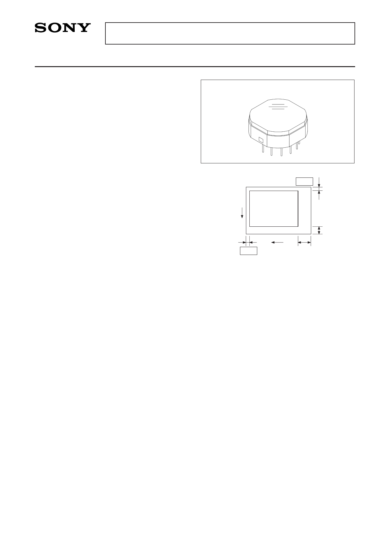
13 pin PCA (Ceramic)
Pin 1
1
Features
• Maximum package dimentions: φ8mm
• High sensitivity and low dark current
• Horizontal register:
3.3 to 5.0V drive
• No voltage adjustment
(Reset gate and substrate bias are not adjusted.)
• Low smear
• Excellent antiblooming characteristics
• Continuous variable-speed shutter
http://www.DataSheet4U.net/
• Ye, Cy, Mg, and G complementary color mosaic filters on chip
V
2
H 25
Pin 8
Optical black position
(Top View)
12
Device Structure
• Interline CCD image sensor
• Image size:
• Number of effective pixels:
• Total number of pixels:
• Chip size:
• Unit cell size:
• Optical black:
• Number of dummy bits:
• Substrate material:
Diagonal 4.5mm (Type 1/4)
510 (H) × 492 (V) approx. 250K pixels
537 (H) × 505 (V) approx. 270K pixels
4.47mm (H) × 3.80mm (V)
7.15µm (H) × 5.55µm (V)
Horizontal (H) direction: Front 2 pixels, rear 25 pixels
Vertical (V) direction: Front 12 pixels, rear 1 pixel
Horizontal 16
Vertical 1 (even fields only)
Silicon
Sony reserves the right to change products and specifications without prior notice. This information does not convey any license by
any implication or otherwise under any patents or other right. Application circuits shown, if any, are typical examples illustrating the
operation of the devices. Sony cannot assume responsibility for any problems arising out of the use of these circuits.
–1–
E95806E99
datasheet pdf - http://www.DataSheet4U.net/
1 page 
ICX086AKB
Drive Clock Waveform Conditions
(1) Readout clock waveform
100%
90%
II II
10%
0%
tr
(2) Vertical transfer clock waveform
Vφ1
VVT
twh
tf
Vφ3
φM
φM
2
0V
VVH1
VVHH
VVH
VVHH
VVHL
VVHL
VVHL
VVHH
VVHH
VVH3
VVHL
VVH
VVL1
VVLH
VVLL
VVL
Vφ2
VVHH
VVH2 VVHL
VVHH
VVH
VVHL
VVL3
http://www.DataSheet4U.net/
VVL
Vφ4
VVH
VVHH
VVLH
VVLL
VVHH
VVHL
VVHL
VVH4
VVL2VVLH
VVLL
VVL
VVH = (VVH1 + VVH2) / 2
VVL = (VVL3 + VVL4) / 2
VφV = VVHn – VVLn (n = 1 to 4)
VVLH
VVLL
VVL4
–5–
VVL
datasheet pdf - http://www.DataSheet4U.net/
5 Page 
ICX086AKB
7. Dark signal shading
After measuring 6, measure the maximum (Ydmax [mV]) and minimum (Ydmin [mV]) values of the Y signal
output and substitute the values into the following formula.
∆Ydt = Ydmax – Ydmin [mV]
8. Flicker
1) Fy
Set to standard imaging condition II. Adjust the luminous intensity so that the average value of the Y signal
output is 200mV, and then measure the difference in the signal level between fields (∆Yf [mV]). Then
substitute the value into the following formula.
Fy = (∆Yf/200) × 100 [%]
2) Fcr, Fcb
Set to standard imaging condition II. Adjust the luminous intensity so that the average value of the Y signal
output is 200mV, insert an R or B filter, and then measure both the difference in the signal level between
fields of the chroma signal (∆Cr, ∆Cb) as well as the average value of the chroma signal output (CAr,
CAb). Substitute the values into the following formula.
Fci = (∆Ci/CAi) × 100 [%] (i = r, b)
9. Line crawls
Set to standard imaging condition II. Adjust the luminous intensity so that the average value of the Y signal
output is 200mV, and then insert a white subject and R, G, and B filters and measure the difference
between Y signal lines for the same field (∆Ylw, ∆Ylr, ∆Ylg,http://www.DataSheet4U.net/ ∆Ylb [mV]). Substitute the values into the
following formula.
Lci = (∆Yli/200) × 100 [%] (i = w, r, g, b)
10. Lag
Adjust the Y signal output value generated by strobe light to 200mV. After setting the strobe light so that it
strobes with the following timing, measure the residual signal (Ylag). Substitute the value into the following
formula.
Lag = (Ylag/200) × 100[%]
FLD
V1
Strobe light
timing
Output
Light
Y signal output 200mV Ylag (lag)
– 11 –
datasheet pdf - http://www.DataSheet4U.net/
11 Page | ||
| Páginas | Total 17 Páginas | |
| PDF Descargar | [ Datasheet ICX086AKB.PDF ] | |
Hoja de datos destacado
| Número de pieza | Descripción | Fabricantes |
| ICX086AK | CCD Image Sensor | Sony |
| ICX086AKB | CCD Image Sensor | Sony |
| Número de pieza | Descripción | Fabricantes |
| SLA6805M | High Voltage 3 phase Motor Driver IC. |
Sanken |
| SDC1742 | 12- and 14-Bit Hybrid Synchro / Resolver-to-Digital Converters. |
Analog Devices |
|
DataSheet.es es una pagina web que funciona como un repositorio de manuales o hoja de datos de muchos de los productos más populares, |
| DataSheet.es | 2020 | Privacy Policy | Contacto | Buscar |