|
|
PDF FP2189 Data sheet ( Hoja de datos )
| Número de pieza | FP2189 | |
| Descripción | 1 Watt GaAs HFET | |
| Fabricantes | TriQuint Semiconductor | |
| Logotipo | ||
Hay una vista previa y un enlace de descarga de FP2189 (archivo pdf) en la parte inferior de esta página. Total 12 Páginas | ||
|
No Preview Available !
FP2189
1-Watt HFET
Product Features
• 50 – 4000 MHz
• +30 dBm P1dB
• +43 dBm Output IP3
• High Drain Efficiency
• 18.5 dB Gain @ 900 MHz
• Lead-free/Green/RoHS-compliant
SOT-89 Package
• MTTF >100 Years
Applications
• Mobile Infrastructure
• CATV / DBS
• W-LAN / ISM
• RFID
• Defense / Homeland Security
• Fixed Wireless
Product Description
The FP2189 is a high performance 1-Watt HFET
(Heterostructure FET) in a low-cost SOT-89 surface-
mount package. This device works optimally at a drain
bias of +8 V and 250 mA to achieve +43 dBm output IP3
performance and an output power of +30 dBm at 1-dB
compression, while providing 18.5 dB gain at 900 MHz.
The device conforms to WJ Communications’ long
history of producing high reliability and quality
components. The FP2189 has an associated MTTF of
greater than 100 years at a mounting temperature of 85 °C
and is available in both the standard SOT-89 package and
the environmentally-friendly lead-free/green/RoHS-
compliant and green SOT-89 package. All devices are
100% RF & DC tested.
The product is targeted for use as driver amplifiers for
wireless infrastructure where high performance and high
efficiency are required.
Functional Diagram
GND
4
1
RF IN
2
GND
3
RF OUT
Function
Input / Gate
Output / Drain
Ground
Pin No.
1
3
2, 4
Specifications
Typical Performance (5)
DC Parameter
Saturated Drain Current, Idss (1)
Transconductance, Gm
Pinch Off Voltage, Vp (2)
RF Parameter (3)
Operational Bandwidth
Test Frequency
Small Signal Gain
SS Gain (50 Ω, unmatched)
Maximum Stable Gain
Output P1dB
Output IP3 (4)
Noise Figure
Drain Bias
Units
mA
mS
V
Units
MHz
MHz
dB
dB
dB
dBm
dBm
dB
Min Typ Max
445 615 705
280
-2.1
Min Typ Max
50 4000
800
18.5
15 21
24
+30
+43
4.5
+8V @ 250 mA
Parameter
Frequency
Gain
www.DataSheet.net/
Input Return Loss
Output Return Loss
Output P1dB
Output IP3 (4)
Noise Figure
IS-95 Channel Power
@ -45 dBc ACPR
W-CDMA Ch. Power
@ -45 dBc ACLR
Drain Voltage
Drain Current
Units
MHz
dB
dB
dB
dBm
dBm
dB
dBm
V
mA
915
18.7
21
8.3
+30.2
+42.8
4.5
Typical
1960 2140
15.6 14.4
14.6 23
12 11.5
+30.4 +30.6
+43.5 +43.9
3.4 4.5
2450
13.0
26
9.6
+31.2
+45.3
+24.5 +23.8
+22.2
+8
250
5. Typical parameters represent performance in a tuned application circuit.
1. Idss is measured with Vgs = 0 V, Vds = 3 V.
2. Pinch-off voltage is measured when Ids = 2.4 mA.
3. Test conditions unless otherwise noted: T = 25 ºC, VDS = 8 V, IDQ = 250 mA in an application circuit
with ZL = ZLOPT, ZS = ZSOPT (optimized for output power).
4. 3OIP measured with two tones at an output power of +15 dBm/tone separated by 1 MHz. The
suppression on the largest IM3 product is used to calculate the 3OIP using a 2:1 rule.
Absolute Maximum Rating
Parameter
Rating
Storage Temperature
-55 to +125 °C
DC Power
4.0 W
RF Input Power (continuous)
6 dB above Input P1dB
Drain to Gate Voltage, Vdg
Junction Temperature
+16 V
+160 °C
Thermal Resistance
30 °C / W
Operation of this device above any of these parameters may cause permanent damage.
Ordering Information
Part No.
FP2189-G
FP2189-PCB900S
FP2189-PCB1900S
FP2189-PCB2140S
Description
1 -Watt HFET
(lead-free/green/RoHS-compliant SOT-89 package)
870 – 960 MHz Application Circuit
1930 – 1990 MHz Application Circuit
2110 – 2170 MHz Application Circuit
Specifications and information are subject to change without notice.
WJ Communications, Inc • Phone 1-800-WJ1-4401 • FAX: 408-577-6621 • e-mail: [email protected] • Web site: www.wj.com, www.TriQuint.com
Page 1 of 12 January 2008
Datasheet pdf - http://www.DataSheet4U.co.kr/
1 page 
FP2189
1-Watt HFET
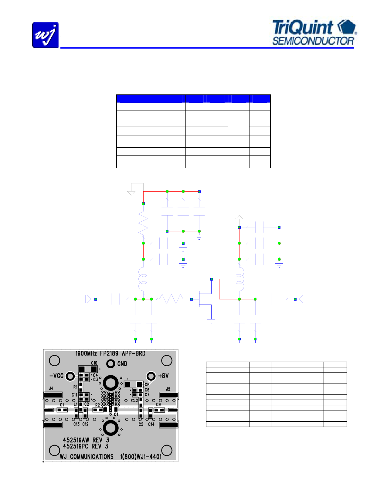
Application Circuit: 1930 – 1990 MHz (FP2189-PCB1900S)
The application circuit is matched for output power.
Typical RF Performance
Drain Bias = +8 V, Ids = 250 mA, 25 °C
Frequency
MHz 1930 1960
S21 – Gain
dB 15.6 15.6
S11 – Input Return Loss
dB -15.4 -14.6
S22 – Output Return Loss dB -12 -12
Output P1dB
dBm +30.2 +30.4
Output IP3
(+15 dBm / tone, 1 MHz spacing)
dBm
+43.5
Noise Figure
dB 3.4 3.4
IS-95 Channel Power
@ -45 dBc ACPR
dBm
+23.8
1990
15.4
-13.2
-12
+30.5
3.6
-Vgg
CAP
ID=C3
CAP
ID=C4
CAP
ID=C10
C=33 pF C=1000 pF C=DNP pF
PORT
P=1
Z=50 Ohm
RES
ID=R1
R=20 Ohm
CAP
I D=C11
C=DNP pF
CAP
I D=C2
C=2.4 pF
CAP
ID=C1
C=33 pF
IND
ID=L1
L=10 nH
RES
ID=R2
R=5.1 Ohm
Vds=8V @ 250 mA
CAP
ID=C8
C=10000 pF
CAP
ID=C6
C=1000 pF
www.DataSheet.net/
CAP
ID=C7
SUBCKT C=33 pF
ID=Q1
NET="FP2189"
2
IND
ID=L2
L=22 nH
1
CAP
ID=C9
C=33 pF
PORT
P=2
Z=50 Ohm
CAP
ID=C13
C=2.4 pF
CAP
ID=C12
C=DNP pF
CAP
I D=C5
C=DNP pF
CAP
ID=C14
C=1.5 pF
Ref. Desig.
C1, C3, C7, C9
C2, C13
C4, C6
C8
C14
L1
L2
R1
R2
Q1
C5, C10, C11, C12
Bill of Materials
Value
100 pF
Part style
Chip capacitor
2.4 pF Chip capacitor
1000 pF Chip capacitor
0.1 μF Chip capacitor
1.5 pF Chip capacitor
10 nH
Multilayer chip inductor
22 nH
Multilayer chip inductor
20 Ω
Chip resistor
5.1 Ω
Chip resistor
FP2189 WJ 1W HFET
Do Not Place
Size
0603
0603
0603
1206
0603
0603
0603
0603
0603
SOT-89
14 mil GETEKTM ML200DSS (εr = 4.2)
The main microstrip line has a line impedance of 50 Ω.
Specifications and information are subject to change without notice.
WJ Communications, Inc • Phone 1-800-WJ1-4401 • FAX: 408-577-6621 • e-mail: [email protected] • Web site: www.wj.com, www.TriQuint.com
Page 5 of 12 January 2008
Datasheet pdf - http://www.DataSheet4U.co.kr/
5 Page 
FP2189
1-Watt HFET
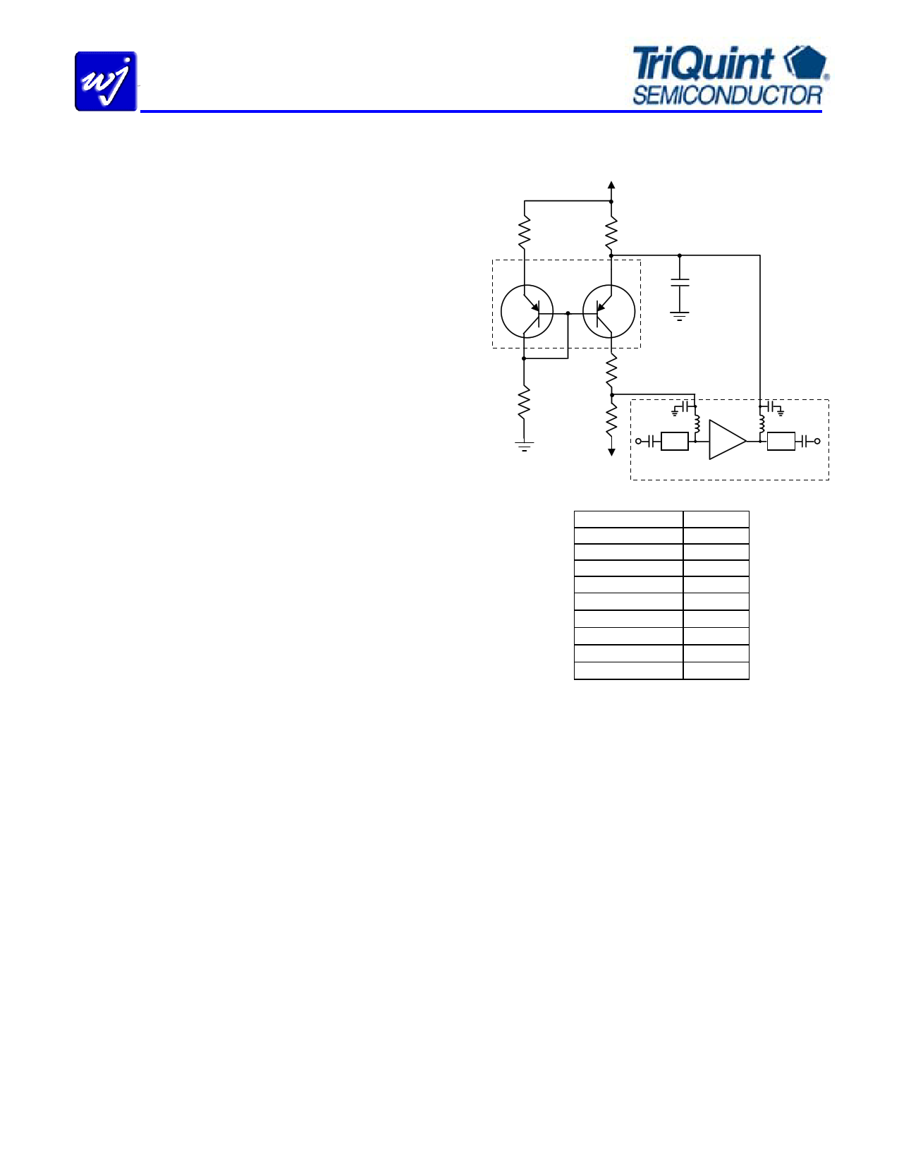
Application Note: Constant-Current Active-Biasing
Special attention should be taken to properly bias the FP2189.
Power supply sequencing is required to prevent the device from
operating at 100% Idss for a prolonged period of time and possibly
causing damage to the device. It is recommended that for the safest
operation, the negative supply be “first on and last off.” With a
negative gate voltage present, the drain voltage can then be applied
to the device. The gate voltage can then be adjusted to have the
device be used at the proper quiescent bias condition.
An optional active-bias current mirror is recommended for use with
the application circuits shown in this datasheet. Generally in a
laboratory environment, the gate voltage is adjusted until the drain
draws the recommended operating current. The gate voltage
required can vary slightly from device to device because of device
pinchoff variation, while also varying slightly over temperature.
The active-bias circuit, shown on the right, uses dual PNP transistors
to provide a constant drain current into the FP2189, while also
eliminating the effects of pinchoff variation. This configuration is
best suited for applications where the intended output power level of
the amplifier is backed off at least 6 dB away from its compression
point. With the implementation of the circuit, lower P1dB values
may be measured for a Class-AB amplifier, where the device will
attempt to source more drain current while the circuit tries to provide
a constant drain current. The circuit should be connected directly in
line with where the voltage supplies would be normally connected
with the amplifier circuit, as shown the diagram. Any requiredwww.DataSheet.net/
matching circuitry remains the same, although it is not shown in the
diagram. This recommended active-bias constant-current circuit
adds 7 components to the parts count for implementation, but should
cost only an extra $0.144 to realize ($0.10 for U1, $0.0029 for R1,
R3, R4, R5, $0.024 for R2, and $0.0085 for C1).
Temperature compensation is achieved by tracking the voltage
variation with the temperature of the emitter-to-base junction of the
two PNP transistors. As a 1st order approximation, this is achieved
by using matched transistors with approximately the same Ibe
current. Thus the transistor emitter voltage adjusts the HFET gate
voltage so that the device draws a constant current, regardless of the
temperature. A Rohm dual transistor - UMT1N - is recommended
for cost, minimal board space requirements, and to minimize the
variation between the two transistors. Minimizing the variability
between the base-to-emitter junctions allow more accuracy in setting
the current draw. More details can be found in a separate application
note “Active-bias Constant-current Source Recommended for
HFETs” found on the WJ website.
+Vdd
R1 R2
U1
4 Rohm UMT1N 1
25
C1
.01 μF
3
R3
6
R4
1 kΩ
R5
-Vgg
RF IN
M.N.
DUT
RF OUT
M.N.
HFET Application Circuit
Parameter
Pos Supply, Vdd
Neg Supply, Vgg
Vds
Ids
R1
R2
R3
R4
R5
FP2189
+8 V
-5 V
+7.75 V
250 mA
62 Ω
1.0 Ω
1.8 kΩ
1 kΩ
1 kΩ
*R2 should be of size 0805 to dissipate 0.0625 Watts.
This should be of 1% tolerance. Two 2.0 Ω resistors in
parallel of size 0603 can also be used.
Specifications and information are subject to change without notice.
WJ Communications, Inc • Phone 1-800-WJ1-4401 • FAX: 408-577-6621 • e-mail: [email protected] • Web site: www.wj.com, www.TriQuint.com
Page 11 of 12 January 2008
Datasheet pdf - http://www.DataSheet4U.co.kr/
11 Page | ||
| Páginas | Total 12 Páginas | |
| PDF Descargar | [ Datasheet FP2189.PDF ] | |
Hoja de datos destacado
| Número de pieza | Descripción | Fabricantes |
| FP2189 | high performance 1-Watt HFET (Heterostructure FET) in a low-cost SOT-89 surfacemount | ETC |
| FP2189 | 1 Watt GaAs HFET | TriQuint Semiconductor |
| FP2189-PCB1900S | high performance 1-Watt HFET (Heterostructure FET) in a low-cost SOT-89 surfacemount | ETC |
| FP2189-PCB2140S | high performance 1-Watt HFET (Heterostructure FET) in a low-cost SOT-89 surfacemount | ETC |
| Número de pieza | Descripción | Fabricantes |
| SLA6805M | High Voltage 3 phase Motor Driver IC. |
Sanken |
| SDC1742 | 12- and 14-Bit Hybrid Synchro / Resolver-to-Digital Converters. |
Analog Devices |
|
DataSheet.es es una pagina web que funciona como un repositorio de manuales o hoja de datos de muchos de los productos más populares, |
| DataSheet.es | 2020 | Privacy Policy | Contacto | Buscar |
