|
|
PDF GS8170DD36C-300 Data sheet ( Hoja de datos )
| Número de pieza | GS8170DD36C-300 | |
| Descripción | Double Data Rate SigmaRAM | |
| Fabricantes | GSI Technology | |
| Logotipo |  |
|
Hay una vista previa y un enlace de descarga de GS8170DD36C-300 (archivo pdf) en la parte inferior de esta página. Total 29 Páginas | ||
|
No Preview Available !
GS8170DD36C-333/300/250/200
209-Bump BGA
Commercial Temp
Industrial Temp
18Mb Σ1x2Lp CMOS I/O
Double Data Rate SigmaRAM™
200 MHz–333 MHz
1.8 V VDD
1.8 V I/O
Features
• Double Data Rate Read and Write mode
• Late Write; Pipelined read operation
• JEDEC-standard SigmaRAM™ pinout and package
• 1.8 V +150/–100 mV core power supply
• 1.8 V CMOS Interface
• ZQ controlled user-selectable output drive strength
• Dual Cycle Deselect
• Burst Read and Write option
• Fully coherent read and write pipelines
• Echo Clock outputs track data output drivers
• 2 user-programmable chip enable inputs
• IEEE 1149.1 JTAG-compliant Serial Boundary Scan
• 209-bump, 14 mm x 22 mm, 1 mm bump pitch BGA package
• Pin-compatible with future 36Mb, 72Mb, and 144Mb
devices
SigmaRAM Family Overview
GS8170DD36 SigmaRAMs are built in compliance with the
SigmaRAM pinout standard for synchronous SRAMs. They
are 18,874,368-bit (18Mb) SRAMs. This family of wide, very
low voltage CMOS I/O SRAMs is designed to operate at the
speeds needed to implement economical high performance
networking systems.
ΣRAMs are offered in a number of configurations including
Late Write, Double Late Write, and Double Data Rate (DDR).
The logical differences between the protocols employed by
these RAMs mainly involve various approaches to write
cueing and data transfer rates. The ΣRAM™ family standard
allows a user to implement the interface protocol best suited to
the task at hand.
Functional Description
Because SigmaRAMs are synchronous devices, address data
inputs and read/write control inputs are captured on the rising
edge of the input clock. Write cycles are internally self-timed
and initiated by the rising edge of the clock input. This feature
eliminates complex off-chip write pulse generation required by
asynchronous SRAMs and simplifies input signal timing. In
DDR mode the device captures Data In on both rising and
falling edges of clock and drives data on both clock edges as
well.
Because the DDR ΣRAM always transfers data in two halves,
A0 is internally set to 0 for the first half of each read or write
transfer, and automatically incremented to 1 for the falling
edge transfer. The address field of a DDR ΣRAM is always
one address pin less than the advertised index depth (e.g., the
512k x 36 has a 512k addressable index).
www.DataSheet.co.kr
ΣRAMs support pipelined reads utilizing a rising-edge-
triggered output register. DDR ΣRAMs incorporate rising-
and falling-edge-triggered output registers. They also utilize a
Dual Cycle Deselect (DCD) output deselect protocol.
ΣRAMs are implemented with high performance CMOS
technology and are packaged in a 209-bump BGA.
Parameter Synopsis
Key Fast Bin Specs
Cycle Time
Access Time
Symbol
tKHKH
tKHQV
- 333
3.0 ns
1.8 ns
Rev: 2.03 1/2005
1/29
Specifications cited are subject to change without notice. For latest documentation see http://www.gsitechnology.com.
© 2002, GSI Technology, Inc.
Datasheet pdf - http://www.DataSheet4U.net/
1 page 
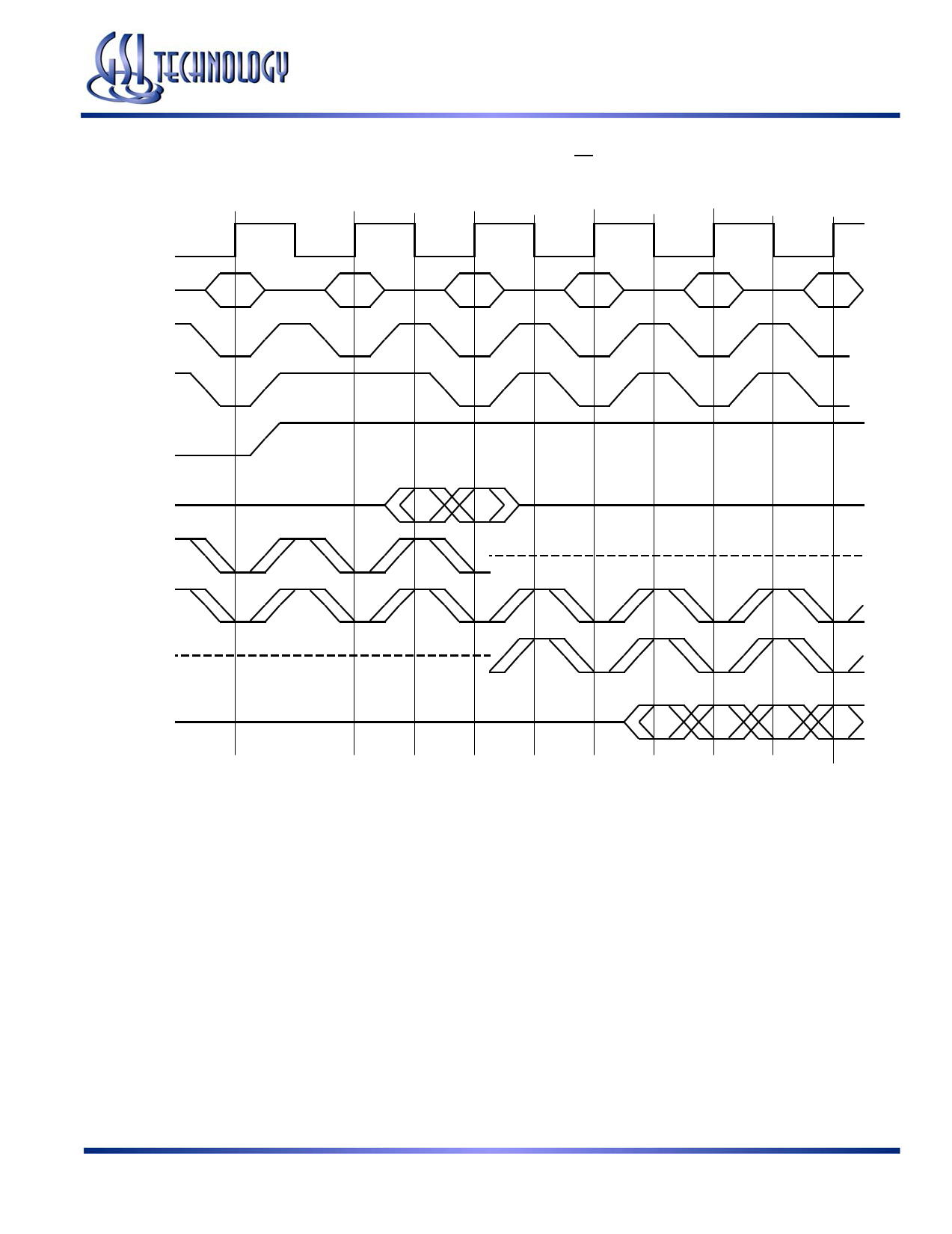
CK
Address
ADV
/E1
/W
DQ
CQ
Read
A
GS8170DD36C-333/300/250/200
SigmaRAM Double Data Rate Read and Write
Deselect
W rite
Read
Read
BCDEF
QA0 QA1
DC0 DC1
QD0 QD1
Key
Hi-Z
www.DataSheet.co.kr
Access
Rev: 2.03 1/2005
5/29
Specifications cited are subject to change without notice. For latest documentation see http://www.gsitechnology.com.
© 2002, GSI Technology, Inc.
Datasheet pdf - http://www.DataSheet4U.net/
5 Page 
GS8170DD36C-333/300/250/200
SigmaRAM DDR Bank Switch with E1 Deselect
Read
No Op
Read
Read
Read
CK
Address
A
XX
C
D
E
F
ADV
/E1
/E2 Bank 1
E2 Bank 2
DQ
Bank 1
CQ
Bank 1
QA0 QA1
CQ1 + CQ2
CQ
Bank 2
www.DataSheet.co.kr
DQ
Bank 2
QC0 QC1 QD0
Note: E1\ does not deselect the Echo Clock Outputs. Echo Clock outputs are synchronously deselected by E2 or E3 being sampled false.
QD1
CMOS Output Driver Impedance Control
CMOS I/O SigmaRAMs are supplied with selectable (high or low) impedance output drivers. The ZQ pin allows selection between
SRAM nominal drive strength (ZQ low) for multi-drop bus applications and low drive strength (ZQ high) point-to-point
applications.
Rev: 2.03 1/2005
11/29
Specifications cited are subject to change without notice. For latest documentation see http://www.gsitechnology.com.
© 2002, GSI Technology, Inc.
Datasheet pdf - http://www.DataSheet4U.net/
11 Page | ||
| Páginas | Total 29 Páginas | |
| PDF Descargar | [ Datasheet GS8170DD36C-300.PDF ] | |
Hoja de datos destacado
| Número de pieza | Descripción | Fabricantes |
| GS8170DD36C-300 | Double Data Rate SigmaRAM | GSI Technology |
| Número de pieza | Descripción | Fabricantes |
| SLA6805M | High Voltage 3 phase Motor Driver IC. |
Sanken |
| SDC1742 | 12- and 14-Bit Hybrid Synchro / Resolver-to-Digital Converters. |
Analog Devices |
|
DataSheet.es es una pagina web que funciona como un repositorio de manuales o hoja de datos de muchos de los productos más populares, |
| DataSheet.es | 2020 | Privacy Policy | Contacto | Buscar |
