|
|
|
PDF ZXLD1352 Data sheet ( Hoja de datos )
| Número de pieza | ZXLD1352 | |
| Descripción | 350mA LED driver | |
| Fabricantes | Zetex Semiconductors | |
| Logotipo | ||
Hay una vista previa y un enlace de descarga de ZXLD1352 (archivo pdf) en la parte inferior de esta página. Total 22 Páginas | ||
|
No Preview Available !
www.DataSheet.co.kr
A Product Line of
Diodes Incorporated
ZXLD1352
350mA LED driver with internal switch and enhanced PWM dimming
range
Description
The ZXLD1352 is a continuous mode
inductive step-down converter, designed for
driving single or multiple series connected
LEDs efficiently from a voltage source higher
than the LED voltage. The device operates
from an input supply between 7V and 30V and
provides an externally adjustable output
current of up to 350mA. Depending upon
supply voltage and external components, this
can provide up to 8 watts of output power.
The ZXLD1352 includes the output switch and
a high-side output current sensing circuit,
which uses an external resistor to set the
nominal average output current.
The ADJ pin will accept either a DC voltage or a
PWM waveform. DC voltages between 0.3V and
2.5V allow adjustment of output current from
25% to 200% of nominal. 1000:1 adjustment of
output current is possible using PWM control.
Applying a voltage of 0.2V or lower to the ADJ
pin turns the output off and switches the device
into a low current standby state.
The device is assembled in a TSOT23-5 pin
package.
Output current can be adjusted above, or
below the set value, by applying an external
control signal to the 'ADJ' pin.
Features
Applications
• Simple low parts count
• Internal 30V NDMOS switch
• 350mA output current
• Single pin on/off and brightness control
using DC voltage or PWM
• 1000:1 PWM dimming range
• Soft-start
• High efficiency (up to 95%(*))
• Wide input voltage range: 7V to 30V
• 40V transient capability
• Low voltage halogen replacement LEDs
• Automotive lighting
• Low voltage industrial lighting
• LED back-up lighting
• Illuminated signs
• Output shutdown
• Up to 1MHz switching frequency
• Inherent open-circuit LED protection
• Typical 4% output current accuracy
(*) Using standard external components as specified under electrical characteristics. Efficiency is dependent upon the
number of LEDs driven and on external component types and values.
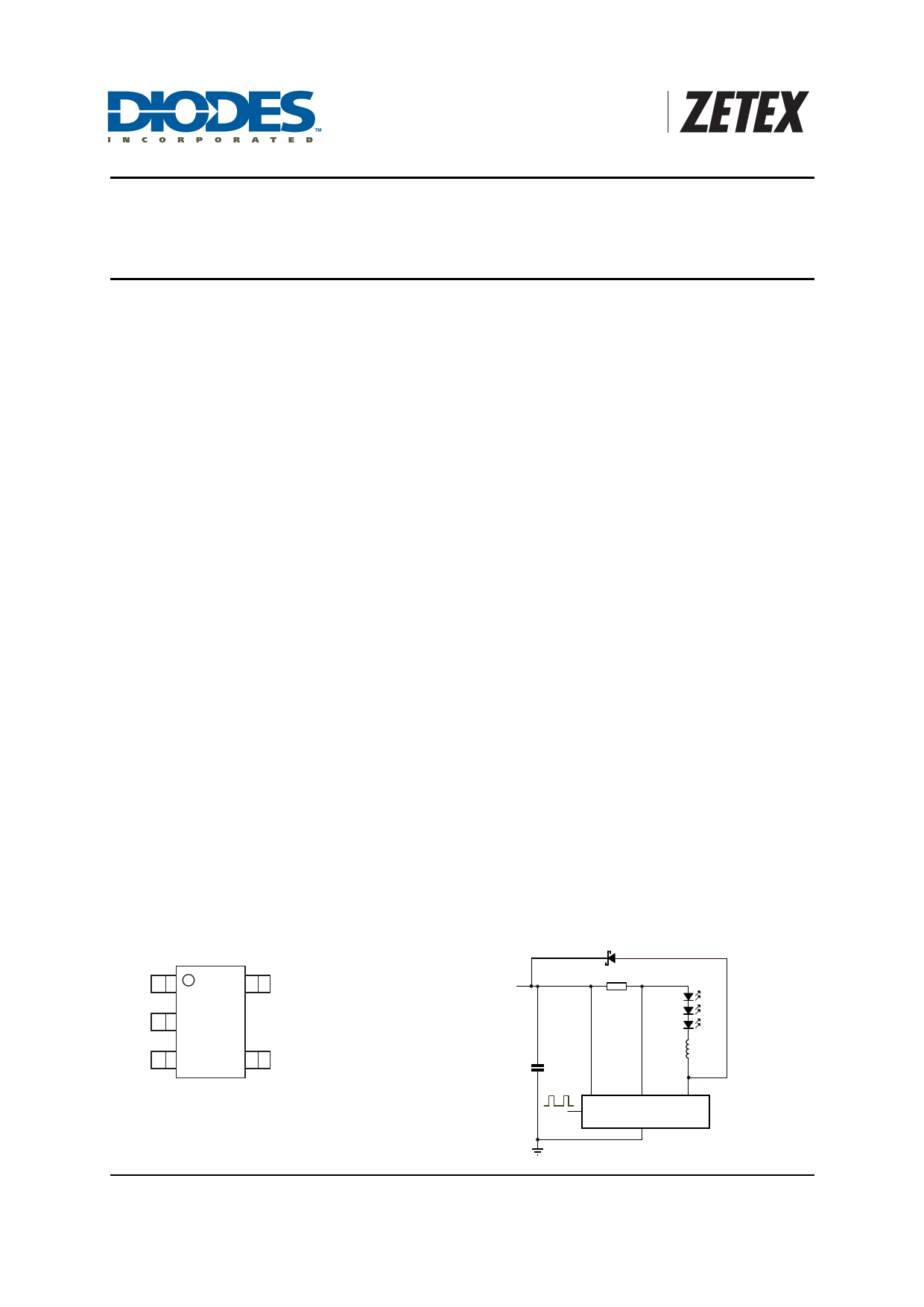
Pin connections
Typical application circuit
LX 1
5 VIN
VIN
(12V - 30V)
D1
ZLLS1000
Rs
0.33
GND 2
ADJ 3
4 ISENSE
TSOT23-5
Top view
C1 1F
PWM
VIN
ADJ
GND
L1 47H
ISENSE
ZXLD1352
GND
LX
Issue 1 - August 2008
© Diodes Incorporated 2008
1
www.zetex.com
www.diodes.com
Datasheet pdf - http://www.DataSheet4U.net/
1 page 
www.DataSheet.co.kr
ZXLD1352
Device description
The device, in conjunction with the coil (L1) and current sense resistor (RS), forms a self-oscillating
continuous-mode buck converter.
Device operation (Refer to block diagram and Figure 1 - Operating waveforms)
Operation can be best understood by assuming that the ADJ pin of the device is unconnected and
the voltage on this pin (VADJ) appears directly at the (+) input of the comparator.
When input voltage VIN is first applied, the initial current in L1 and RS is zero and there is no
output from the current sense circuit. Under this condition, the (-) input to the comparator is at
ground and its output is high. This turns MN on and switches the LX pin low, causing current to
flow from VIN to ground, via RS, L1 and the LED(s). The current rises at a rate determined by VIN
and L1 to produce a voltage ramp (VSENSE) across RS. The supply referred voltage VSENSE is
forced across internal resistor R1 by the current sense circuit and produces a proportional current
in internal resistors R2 and R3. This produces a ground referred rising voltage at the (-) input of
the comparator. When this reaches the threshold voltage (VADJ), the comparator output switches
low and MN turns off. The comparator output also drives another NMOS switch, which bypasses
internal resistor R3 to provide a controlled amount of hysteresis. The hysteresis is set by R3 to be
nominally 15% of VADJ.
When MN is off, the current in L1 continues to flow via D1 and the LED(s) back to VIN. The current
decays at a rate determined by the LED and diode forward voltages to produce a falling voltage
at the input of the comparator. When this voltage returns to VADJ, the comparator output switches
high again. This cycle of events repeats, with the comparator input ramping between limits of
VADJ ± 15%.
Switching thresholds
With VADJ =VREF, the ratios of R1, R2 and R3, define an average VSENSE switching threshold of
100mV (measured on the ISENSE pin with respect to VIN). The average output current IOUTnom is
then defined by this voltage and Rs according to:
IOUTnom=100mV/RS
Nominal ripple current is ±15mV/RS
Adjusting output current
The device contains a low pass filter for noise suppression between the ADJ pin and the threshold
comparator and an internal current limiting resistor (50k nom) between ADJ and the internal
reference voltage. This allows the ADJ pin to be overdriven with either DC or PWM signals to
adjust the output current. The filter is first order, comprising one section with a cut-off frequency
of nominally 600kHz.
Details of the different modes of adjusting output current are given in the applications section.
Output shutdown
The ADJ pin drives the shutdown circuit. When the input voltage to this circuit falls below the
threshold (0.2V nom), the internal regulator and the output switch are turned off. The voltage
reference remains powered during shutdown to provide the bias current for the shutdown circuit.
Quiescent supply current during shutdown is nominally 20A and switch leakage is below 1A.
Issue 1 - August 2008
© Diodes Incorporated 2008
5
www.zetex.com
www.diodes.com
Datasheet pdf - http://www.DataSheet4U.net/
5 Page 
www.DataSheet.co.kr
ZXLD1352
Typical operating conditions (continued)
Vref vs Vin over nominal supply voltage range
1.2425
1.242
1.2415
5
10 15 20 25
Vin (V)
500
400
300
200
100
0
0
Supply Current vs Vin (Operating)
5 10 15 20 25
Vin (V)
30
30
Output Current vs VADJ
350
300
250
200 Rs=0.3 Ohm
Rs=0.56 Ohm
150 Rs=1 Ohm
100
50
0
0 0.5 1 1.5 2 2.5 3
VADJ (V)
1.4
1.2
1
0.8
0.6
0.4
0.2
0
0
Vref vs Vin at low supply voltage
12 3 4 56 7 8
Vin (V)
9 10
20
15
10
5
0
0
Supply Current vs Vin (Quiescent)
5 10 15 20 25 30
Vin (V)
Issue 1 - August 2008
© Diodes Incorporated 2008
11
www.zetex.com
www.diodes.com
Datasheet pdf - http://www.DataSheet4U.net/
11 Page | ||
| Páginas | Total 22 Páginas | |
| PDF Descargar | [ Datasheet ZXLD1352.PDF ] | |
Hoja de datos destacado
| Número de pieza | Descripción | Fabricantes |
| ZXLD1350 | 350mA LED driver | Zetex Semiconductors |
| ZXLD1350 | 30V 350mA LED DRIVER | Diodes |
| ZXLD1350Q | AUTOMOTIVE GRADE 350mA BUCK LED DRIVER | Diodes |
| ZXLD1352 | 350mA LED driver | Zetex Semiconductors |
| Número de pieza | Descripción | Fabricantes |
| SLA6805M | High Voltage 3 phase Motor Driver IC. |
Sanken |
| SDC1742 | 12- and 14-Bit Hybrid Synchro / Resolver-to-Digital Converters. |
Analog Devices |
|
DataSheet.es es una pagina web que funciona como un repositorio de manuales o hoja de datos de muchos de los productos más populares, |
| DataSheet.es | 2020 | Privacy Policy | Contacto | Buscar |