|
|
|
PDF FM25W256 Data sheet ( Hoja de datos )
| Número de pieza | FM25W256 | |
| Descripción | 256Kb Wide Voltage SPI F-RAM | |
| Fabricantes | Ramtron | |
| Logotipo | ||
Hay una vista previa y un enlace de descarga de FM25W256 (archivo pdf) en la parte inferior de esta página. Total 13 Páginas | ||
|
No Preview Available !
www.DataSheet.co.kr
Preliminary
FM25W256
256Kb Wide Voltage SPI F-RAM
Features
256K bit Ferroelectric Nonvolatile RAM
• Organized as 32,768 x 8 bits
• High Endurance 100 Trillion (1014) Read/Writes
• 38 Year Data Retention (@ +75ºC)
• NoDelay™ Writes
• Advanced High-Reliability Ferroelectric Process
Very Fast Serial Peripheral Interface - SPI
• Up to 20 MHz Frequency
• Direct Hardware Replacement for EEPROM
• SPI Mode 0 & 3 (CPOL, CPHA=0,0 & 1,1)
Description
The FM25W256 is a 256-kilobit nonvolatile memory
employing an advanced ferroelectric process. A
ferroelectric random access memory or F-RAM is
nonvolatile and performs reads and writes like a
RAM. It provides reliable data retention for 10 years
while eliminating the complexities, overhead, and
system level reliability problems caused by
EEPROM and other nonvolatile memories.
The FM25W256 performs write operations at bus
speed. No write delays are incurred. Data is written to
the memory array immediately after it has been
successfully transferred to the device. The next bus
cycle may commence immediately without the need
for data polling. In addition, the product offers
substantial write endurance compared with other
nonvolatile memories. The FM25W256 is capable of
supporting 1014 read/write cycles, or 100 million
times more write cycles than EEPROM.
These capabilities make the FM25W256 ideal for
nonvolatile memory applications requiring frequent
or rapid writes or low power operation. Examples
range from data collection, where the number of
write cycles may be critical, to demanding industrial
controls where the long write time of EEPROM can
cause data loss.
The FM25W256 provides substantial benefits to
users of serial EEPROM as a hardware drop-in
replacement. The FM25W256 uses the high-speed
SPI bus, which enhances the high-speed write
capability of F-RAM technology. Device
specifications are guaranteed over an industrial
temperature range of -40°C to +85°C.
Write Protection Scheme
• Hardware Protection
• Software Protection
Low Power Operation
• Wide Voltage Operation 2.7V – 5.5V
• 15 µA (typ.) Standby Current
Industry Standard Configurations
• Industrial Temperature -40°C to +85°C
• 8-pin “Green”/RoHS SOIC (-G)
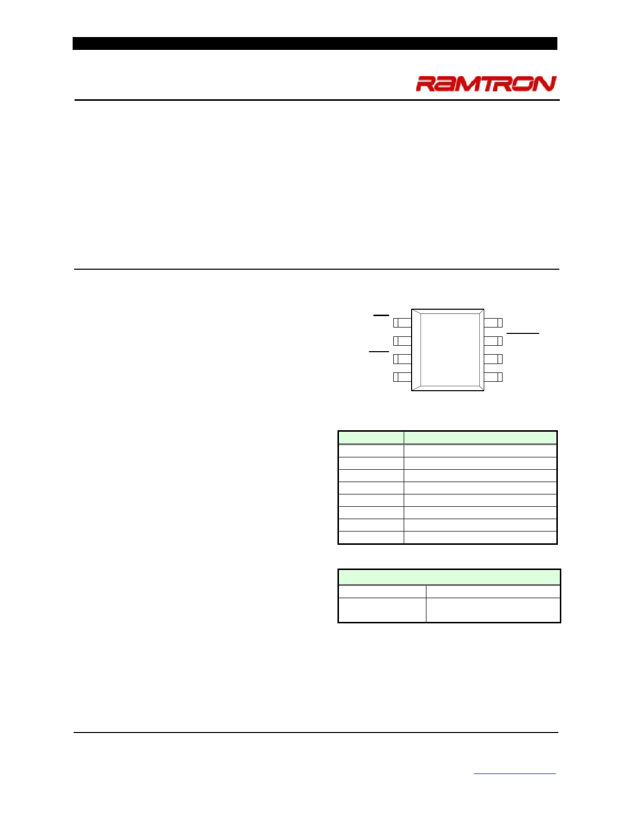
Pin Configuration
CS
SO
WP
VSS
1
2
3
4
8 VDD
7 HOLD
6 SCK
5 SI
Pin Name
/CS
/WP
/HOLD
SCK
SI
SO
VDD
VSS
Function
Chip Select
Write Protect
Hold
Serial Clock
Serial Data Input
Serial Data Output
Supply Voltage (2.7 to 5.5V)
Ground
Ordering Information
FM25W256-G
“Green”/RoHS 8-pin SOIC
FM25W256-GTR “Green”/RoHS 8-pin SOIC,
Tape & Reel
This is a product that has fixed target specifications but are subject
to change pending characterization results.
Rev. 1.3
Feb. 2011
Ramtron International Corporation
1850 Ramtron Drive, Colorado Springs, CO 80921
(800) 545-FRAM, (719) 481-7000
http://www.ramtron.com
Page 1 of 13
Datasheet pdf - http://www.DataSheet4U.net/
1 page 
www.DataSheet.co.kr
FM25W256 - 256Kb SPI F-RAM
Power Up to First Access
The FM25W256 is not accessible for a period of time
(tPU) after power up. Users must comply with the
timing parameter tPU, which is the minimum time
from VDD (min) to the first /CS low.
Data Transfer
All data transfers to and from the FM25W256 occur
in 8-bit groups. They are synchronized to the clock
signal (SCK), and they transfer most significant bit
(MSB) first. Serial inputs are registered on the rising
edge of SCK. Outputs are driven from the falling
edge of SCK.
Command Structure
There are six commands called op-codes that can be
issued by the bus master to the FM25W256. They are
listed in the table below. These op-codes control the
functions performed by the memory. They can be
divided into three categories. First, there are
commands that have no subsequent operations. They
perform a single function such as to enable a write
operation. Second are commands followed by one
byte, either in or out. They operate on the status
register. The third group includes commands for
memory transactions followed by address and one or
more bytes of data.
Table 1. Op-code Commands
Name Description
WREN Set Write Enable Latch
WRDI Write Disable
RDSR Read Status Register
WRSR Write Status Register
READ Read Memory Data
WRITE Write Memory Data
Op-code
0000 0110b
0000 0100b
0000 0101b
0000 0001b
0000 0011b
0000 0010b
WREN – Set Write Enable Latch
The FM25W256 will power up with writes disabled.
The WREN command must be issued prior to any
write operation. Sending the WREN op-code will
allow the user to issue subsequent op-codes for
write operations. These include writing the status
register and writing the memory.
Sending the WREN op-code causes the internal
Write Enable Latch to be set. A flag bit in the status
register, called WEL, indicates the state of the latch.
WEL=1 indicates that writes are permitted.
Attempting to write the WEL bit in the status
register has no effect on the state of this bit.
Completing any write operation will automatically
clear the write-enable latch and prevent further
writes without another WREN command. Figure 5
illustrates the WREN command bus configuration.
WRDI – Write Disable
The WRDI command disables all write activity by
clearing the Write Enable Latch. The user can verify
that writes are disabled by reading the WEL bit in
the status register and verifying that WEL=0. Figure
6 illustrates the WRDI command bus configuration.
CS
SCK
SI
SO
01 2 3 4 5 6 7
00 00 0 11
Hi-Z
Figure 5. WREN Bus Configuration
0
Rev. 1.3
Feb. 2011
Page 5 of 13
Datasheet pdf - http://www.DataSheet4U.net/
5 Page 
www.DataSheet.co.kr
Serial Data Bus Timing
FM25W256 - 256Kb SPI F-RAM
/HOLD Timing
S
C
HOLD
Q
Power Cycle Timing
tHS
tHH
tHS
tHH
tHZ tLZ
Power Cycle Timing (TA = -40° C to + 85° C, VDD = 2.7V to 5.5V unless otherwise specified)
Symbol
Parameter
Min Max Units
tPU VDD(min) to First Access Start
tPD Last Access Complete to VDD(min)
tVR VDD Rise Time
10 - ms
0 - µs
30 - µs/V
tVF VDD Fall Time
100 - µs/V
Notes
1. Slope measured at any point on VDD waveform.
Notes
1
1
Rev. 1.3
Feb. 2011
Page 11 of 13
Datasheet pdf - http://www.DataSheet4U.net/
11 Page | ||
| Páginas | Total 13 Páginas | |
| PDF Descargar | [ Datasheet FM25W256.PDF ] | |
Hoja de datos destacado
| Número de pieza | Descripción | Fabricantes |
| FM25W256 | 256-Kbit (32K x 8) Serial (SPI) F-RAM | Cypress Semiconductor |
| FM25W256 | 256Kb Wide Voltage SPI F-RAM | Ramtron |
| Número de pieza | Descripción | Fabricantes |
| SLA6805M | High Voltage 3 phase Motor Driver IC. |
Sanken |
| SDC1742 | 12- and 14-Bit Hybrid Synchro / Resolver-to-Digital Converters. |
Analog Devices |
|
DataSheet.es es una pagina web que funciona como un repositorio de manuales o hoja de datos de muchos de los productos más populares, |
| DataSheet.es | 2020 | Privacy Policy | Contacto | Buscar |