|
|
|
PDF FM25V02 Data sheet ( Hoja de datos )
| Número de pieza | FM25V02 | |
| Descripción | 3V F-RAM Memory | |
| Fabricantes | Ramtron | |
| Logotipo | ||
Hay una vista previa y un enlace de descarga de FM25V02 (archivo pdf) en la parte inferior de esta página. Total 17 Páginas | ||
|
No Preview Available !
www.DataSheet.co.kr
Pre-Production
FM25V02
256Kb Serial 3V F-RAM Memory
Features
256K bit Ferroelectric Nonvolatile RAM
• Organized as 32,768 x 8 bits
• High Endurance 100 Trillion (1014) Read/Writes
• 10 Year Data Retention
• NoDelay™ Writes
• Advanced High-Reliability Ferroelectric Process
Very Fast Serial Peripheral Interface - SPI
• Up to 40 MHz Frequency
• Direct Hardware Replacement for Serial Flash
• SPI Mode 0 & 3 (CPOL, CPHA=0,0 & 1,1)
Write Protection Scheme
• Hardware Protection
• Software Protection
Device ID and Serial Number
• Device ID reads out Manufacturer ID & Part ID
• Unique Serial Number (FM25VN02)
Low Voltage, Low Power
• Low Voltage Operation 2.0V – 3.6V
• 90 µA Standby Current (typ.)
• 5 µA Sleep Mode Current (typ.)
Industry Standard Configurations
• Industrial Temperature -40°C to +85°C
• 8-pin “Green”/RoHS SOIC Package
• 8-pin “Green”/RoHS TDFN Package
Description
The FM25V02 is a 256-kilobit nonvolatile memory
employing an advanced ferroelectric process. A
ferroelectric random access memory or F-RAM is
nonvolatile and performs reads and writes like a
RAM. It provides reliable data retention for 10 years
while eliminating the complexities, overhead, and
system level reliability problems caused by Serial
Flash and other nonvolatile memories.
Unlike Serial Flash, the FM25V02 performs write
operations at bus speed. No write delays are incurred.
Data is written to the memory array immediately
after it has been transferred to the device. The next
bus cycle may commence without the need for data
polling. The product offers very high write
endurance, orders of magnitude more endurance than
Serial Flash. Also, F-RAM exhibits lower power
consumption than Serial Flash.
These capabilities make the FM25V02 ideal for
nonvolatile memory applications requiring frequent
or rapid writes or low power operation. Examples
range from data collection, where the number of
write cycles may be critical, to demanding industrial
controls where the long write time of Serial Flash can
cause data loss.
The FM25V02 provides substantial benefits to users
of Serial Flash as a hardware drop-in replacement.
The devices use the high-speed SPI bus, which
enhances the high-speed write capability of F-RAM
technology. The FM25VN02 is offered with a unique
This is a product in the pre-production phase of development. Device
characterization is complete and Ramtron does not expect to change the
specifications. Ramtron will issue a Product Change Notice if any
specification changes are made.
Rev. 2.0
May 2010
serial number that is read-only and can be used to
identify a board or system. Both devices incorporate
a read-only Device ID that allows the host to
determine the manufacturer, product density, and
product revision. The devices are guaranteed over an
industrial temperature range of -40°C to +85°C.
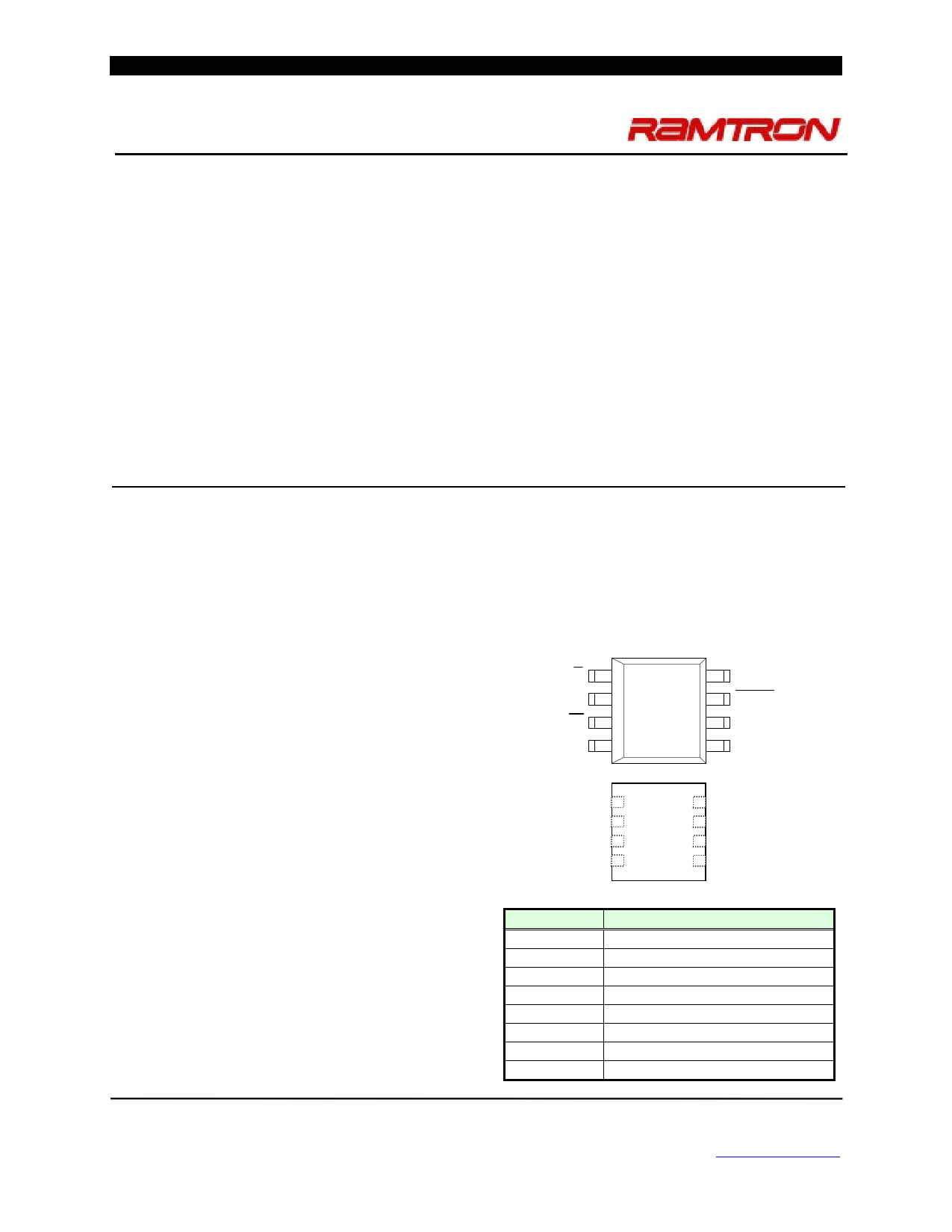
Pin Configuration
S
Q
W
VSS
1
2
3
4
8 VDD
7 HOLD
6C
5D
/S 1
Q2
/W 3
VSS 4
8 VDD
7 /HOLD
6C
5D
Pin Name
/S
/W
/HOLD
C
D
Q
VDD
VSS
Top View
Function
Chip Select
Write Protect
Hold
Serial Clock
Serial Data Input
Serial Data Output
Supply Voltage
Ground
Ramtron International Corporation
1850 Ramtron Drive, Colorado Springs, CO 80921
(800) 545-FRAM, (719) 481-7000
http://www.ramtron.com
Page 1 of 17
Datasheet pdf - http://www.DataSheet4U.net/
1 page 
www.DataSheet.co.kr
Power Up to First Access
The FM25V02 is not accessible for a period of time
(tPU) after power up. Users must comply with the
timing parameter tPU, which is the minimum time
from VDD (min) to the first /S low.
Data Transfer
All data transfers to and from the FM25V02 occur in
8-bit groups. They are synchronized to the clock
signal (C), and they transfer most significant bit
(MSB) first. Serial inputs are registered on the rising
edge of C. Outputs are driven from the falling edge of
clock C.
Command Structure
There are ten commands called op-codes that can be
issued by the bus master to the FM25V02. They are
listed in the table below. These op-codes control the
functions performed by the memory. They can be
divided into three categories. First, there are
commands that have no subsequent operations. They
perform a single function, such as to enable a write
operation. Second are commands followed by one
byte, either in or out. They operate on the Status
Register. The third group includes commands for
memory transactions followed by address and one or
more bytes of data.
Table 1. Op-code Commands
Name Description
WREN Set Write Enable Latch
WRDI Write Disable
RDSR Read Status Register
WRSR Write Status Register
READ Read Memory Data
FSTRD Fast Read Memory Data
WRITE Write Memory Data
SLEEP Enter Sleep Mode
RDID Read Device ID
SNR
Read S/N
Op-code
0000 0110b
0000 0100b
0000 0101b
0000 0001b
0000 0011b
0000 1011b
0000 0010b
1011 1001b
1001 1111b
1100 0011b
WREN – Set Write Enable Latch
The FM25V02 will power up with writes disabled.
The WREN command must be issued prior to any
write operation. Sending the WREN op-code will
allow the user to issue subsequent op-codes for write
operations. These include writing the Status Register
(WRSR) and writing the memory (WRITE).
Sending the WREN op-code causes the internal Write
Enable Latch to be set. A flag bit in the Status
Register, called WEL, indicates the state of the latch.
WEL=1 indicates that writes are permitted.
Attempting to write the WEL bit in the Status
Register has no effect on the state of this bit.
Completing any write operation will automatically
Rev. 2.0
May 2010
FM25V02 - 256Kb SPI FRAM
clear the write-enable latch and prevent further
writes without another WREN command. Figure 5
below illustrates the WREN command bus
configuration.
S
01234567
C
D 00000110
Q Hi-Z
Figure 5. WREN Bus Configuration
WRDI – Write Disable
The WRDI command disables all write activity by
clearing the Write Enable Latch. The user can verify
that writes are disabled by reading the WEL bit in
the Status Register and verifying that WEL=0.
Figure 6 illustrates the WRDI command bus
configuration.
S
01234567
C
D 00000100
Q Hi-Z
Figure 6. WRDI Bus Configuration
RDSR – Read Status Register
The RDSR command allows the bus master to
verify the contents of the Status Register. Reading
Status provides information about the current state
of the write protection features. Following the
RDSR op-code, the FM25V02 will return one byte
with the contents of the Status Register. The Status
Register is described in detail in the section below.
Page 5 of 17
Datasheet pdf - http://www.DataSheet4U.net/
5 Page 
www.DataSheet.co.kr
FM25V02 - 256Kb SPI FRAM
S
C .......
D C3h
Q
Byte 7
Byte 6
...
Byte 1
Byte 0
Figure 15. Read Serial Number
Endurance
The FM25V02 and FM25VN02 devices are capable
of being accessed at least 1014 times, reads or writes.
An F-RAM memory operates with a read and restore
mechanism. Therefore, an endurance cycle is applied
on a row basis for each access (read or write) to the
memory array. The F-RAM architecture is based on
an array of rows and columns. Rows are defined by
A14-A3 and column addresses by A2-A0. See Block
Diagram (pg 2) which shows the array as 4K rows of
64-bits each. The entire row is internally accessed
once whether a single byte or all eight bytes are read
or written. Each byte in the row is counted only once
in an endurance calculation. The table below shows
endurance calculations for 64-byte repeating loop,
which includes an op-code, a starting address, and a
sequential 64-byte data stream. This causes each byte
to experience one endurance cycle through the loop.
F-RAM read and write endurance is virtually
unlimited even at 40MHz clock rate.
Table 7. Time to Reach 100 Trillion Cycles for Repeating 64-byte Loop
SCK Freq
Endurance
Endurance
Years to Reach
(MHz)
Cycles/sec.
Cycles/year
1014 Cycles
40
74,620
2.35 x 10¹²
42.6
20
37,310
1.18 x 10¹²
85.1
10
18,660
5.88 x 10¹¹
170.2
5
9,330
2.94 x 10¹¹
340.3
Rev. 2.0
May 2010
Page 11 of 17
Datasheet pdf - http://www.DataSheet4U.net/
11 Page | ||
| Páginas | Total 17 Páginas | |
| PDF Descargar | [ Datasheet FM25V02.PDF ] | |
Hoja de datos destacado
| Número de pieza | Descripción | Fabricantes |
| FM25V01 | 128Kb Serial 3V F-RAM Memory | Cypress Semiconductor |
| FM25V01 | 3V F-RAM Memory | Ramtron |
| FM25V01A | 128-Kbit (16K x 8) Serial (SPI) F-RAM | Cypress Semiconductor |
| FM25V02 | 3V F-RAM Memory | Ramtron |
| Número de pieza | Descripción | Fabricantes |
| SLA6805M | High Voltage 3 phase Motor Driver IC. |
Sanken |
| SDC1742 | 12- and 14-Bit Hybrid Synchro / Resolver-to-Digital Converters. |
Analog Devices |
|
DataSheet.es es una pagina web que funciona como un repositorio de manuales o hoja de datos de muchos de los productos más populares, |
| DataSheet.es | 2020 | Privacy Policy | Contacto | Buscar |