|
|
|
PDF DS10CP152Q Data sheet ( Hoja de datos )
| Número de pieza | DS10CP152Q | |
| Descripción | Automotive 1.5 Gbps 2X2 LVDS Crosspoint Switch | |
| Fabricantes | National Semiconductor | |
| Logotipo | ||
Hay una vista previa y un enlace de descarga de DS10CP152Q (archivo pdf) en la parte inferior de esta página. Total 12 Páginas | ||
|
No Preview Available !
www.DataSheet.co.kr
June 3, 2008
DS10CP152Q
Automotive 1.5 Gbps 2X2 LVDS Crosspoint Switch
General Description
The DS10CP152Q is a 1.5 Gbps 2x2 LVDS crosspoint switch
optimized for high-speed signal routing and switching over
lossy FR-4 printed circuit board backplanes and balanced ca-
bles. Fully differential signal paths ensure exceptional signal
integrity and noise immunity. The non-blocking architecture
allows connections of any input to any output or outputs.
Wide input common mode range allows the switch to accept
signals with LVDS, CML and LVPECL levels; the output levels
are LVDS. A very small package footprint requires a minimal
space on the board while the flow-through pinout allows easy
board layout. Each differential input and output is internally
terminated with a 100Ω resistor to lower device return losses,
reduce component count and further minimize board space.
Features
■ AECQ-100 Grade 3
■ DC - 1.5 Gbps low jitter, low skew, low power operation
■ Pin configurable, fully differential, non-blocking
architecture
■ Wide Input Common Mode Voltage Range allows DC-
coupled interface to LVDS, CML and LVPECL drivers
■ On-chip 100Ω input and output termination minimizes
insertion and return losses, reduces component count and
minimizes board space
■ 8 kV ESD on LVDS I/O pins protects adjoining
components
■ Small SOIC-16 space saving package
Applications
■ Automotive display applications
■ Clock and data buffering and muxing
■ SD/HD SDI Routers
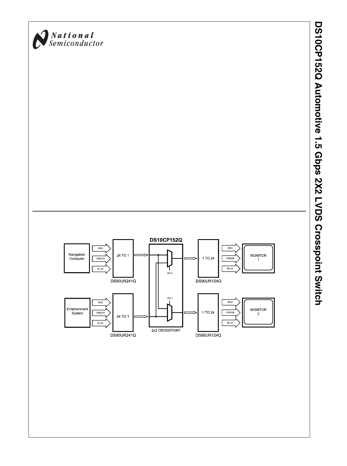
Typical Application
© 2008 National Semiconductor Corporation 300637
30063770
www.national.com
Datasheet pdf - http://www.DataSheet4U.net/
1 page 
www.DataSheet.co.kr
AC Electrical Characteristics
Over recommended operating supply and temperature ranges unless otherwise specified. (Notes 9, 10, 11)
Symbol
Parameter
Conditions
Min Typ
LVDS OUTPUT AC SPECIFICATIONS
tPLHD
tPHLD
Differential Propagation Delay Low to
High
Differential Propagation Delay High to
Low
RL = 100Ω
440
400
tSKD1
Pulse Skew |tPLHD − tPHLD|
(Note 12)
40
tSKD2
Channel to Channel Skew
(Note 13)
25
tSKD3
Part to Part Skew
(Note 14)
45
tLHT Rise Time
tHLT Fall Time
tON Output Enable Time
tOFF Output Disable Time
tSEL Select Time
JITTER PERFORMANCE (Note 11)
RL = 100Ω
170
170
5
3
3
tRJ1
VID = 350 mV
135 MHz
tRJ2
tRJ3
Random Jitter (RMS Value)
VCM = 1.2V
Clock (RZ)
311 MHz
503 MHz
tRJ4 750 MHz
tDJ1
tDJ2 Deterministic Jitter
tDJ3 (Peak-to-Peak Value )
VID = 350 mV
VCM = 1.2V
Clock (RZ)
270 Mbps
622 Mbps
1.06 Gbps
tDJ4 1.5 Gbps
tTJ1
VID = 350 mV
270 Mbps
tTJ2
tTJ3
Total Jitter (Peak to Peak Value)
VCM = 1.2V
PRBS-23 (NRZ)
622 Mbps
1.06 Gbps
tTJ4 1.5 Gbps
0.5
0.5
0.5
0.5
9
7
7
9
0.01
0.01
0.01
0.01
Max
650
650
120
60
190
350
350
20
12
12
1.2
1.2
1.2
1.2
38
36
34
35
0.03
0.04
0.05
0.07
Units
ps
ps
ps
ps
ps
ps
ps
μs
ns
ns
ps
ps
ps
ps
ps
ps
ps
ps
UIP-P
UIP-P
UIP-P
UIP-P
Note 9: The Electrical Characteristics tables list guaranteed specifications under the listed Recommended Operating Conditions except as otherwise modified
or specified by the Electrical Characteristics Conditions and/or Notes. Typical specifications are estimations only and are not guaranteed.
Note 10: Typical values represent most likely parametric norms for VCC = +3.3V and TA = +25°C, and at the Recommended Operation Conditions at the time of
product characterization and are not guaranteed.
Note 11: Specification is guaranteed by characterization and is not tested in production.
Note 12: tSKD1, |tPLHD − tPHLD|, Pulse Skew, is the magnitude difference in differential propagation delay time between the positive going edge and the negative
going edge of the same channel.
Note 13: tSKD2, Channel to Channel Skew, is the difference in propagation delay (tPLHD or tPHLD) among all output channels in Broadcast mode (any one input to
all outputs).
Note 14: tSKD3, Part to Part Skew, is defined as the difference between the minimum and maximum differential propagation delays. This specification applies to
devices at the same VCC and within 5°C of each other within the operating temperature range.
Note 15: Measured on a clock edge with a histogram and an acummulation of 1500 histogram hits. Input stimulus jitter is subtracted geometrically.
Note 16: Tested with a combination of the 1100000101 (K28.5+ character) and 0011111010 (K28.5- character) patterns. Input stimulus jitter is subtracted
algebraically.
Note 17: Measured on an eye diagram with a histogram and an acummulation of 3500 histogram hits. Input stimulus jitter is subtracted.
5 www.national.com
Datasheet pdf - http://www.DataSheet4U.net/
5 Page 
www.DataSheet.co.kr
Physical Dimensions inches (millimeters) unless otherwise noted
Order Number DS10CP152QMA
NS Package Number M16A
11
www.national.com
Datasheet pdf - http://www.DataSheet4U.net/
11 Page | ||
| Páginas | Total 12 Páginas | |
| PDF Descargar | [ Datasheet DS10CP152Q.PDF ] | |
Hoja de datos destacado
| Número de pieza | Descripción | Fabricantes |
| DS10CP152 | DS10CP152 1.5 Gbps 2X2 LVDS Crosspoint Switch (Rev. E) | Texas Instruments |
| DS10CP152 | 1.5 Gbps 2X2 LVDS Crosspoint Switch | National Semiconductor |
| DS10CP152Q | DS10CP152Q Automotive 1.5 Gbps 2X2 LVDS Crosspoint Switch (Rev. E) | Texas Instruments |
| DS10CP152Q | Automotive 1.5 Gbps 2X2 LVDS Crosspoint Switch | National Semiconductor |
| Número de pieza | Descripción | Fabricantes |
| SLA6805M | High Voltage 3 phase Motor Driver IC. |
Sanken |
| SDC1742 | 12- and 14-Bit Hybrid Synchro / Resolver-to-Digital Converters. |
Analog Devices |
|
DataSheet.es es una pagina web que funciona como un repositorio de manuales o hoja de datos de muchos de los productos más populares, |
| DataSheet.es | 2020 | Privacy Policy | Contacto | Buscar |