|
|
|
PDF KS8999 Data sheet ( Hoja de datos )
| Número de pieza | KS8999 | |
| Descripción | Integrated 9-Port 10/100 Switch | |
| Fabricantes | Micrel Semiconductor | |
| Logotipo | ||
Hay una vista previa y un enlace de descarga de KS8999 (archivo pdf) en la parte inferior de esta página. Total 53 Páginas | ||
|
No Preview Available !
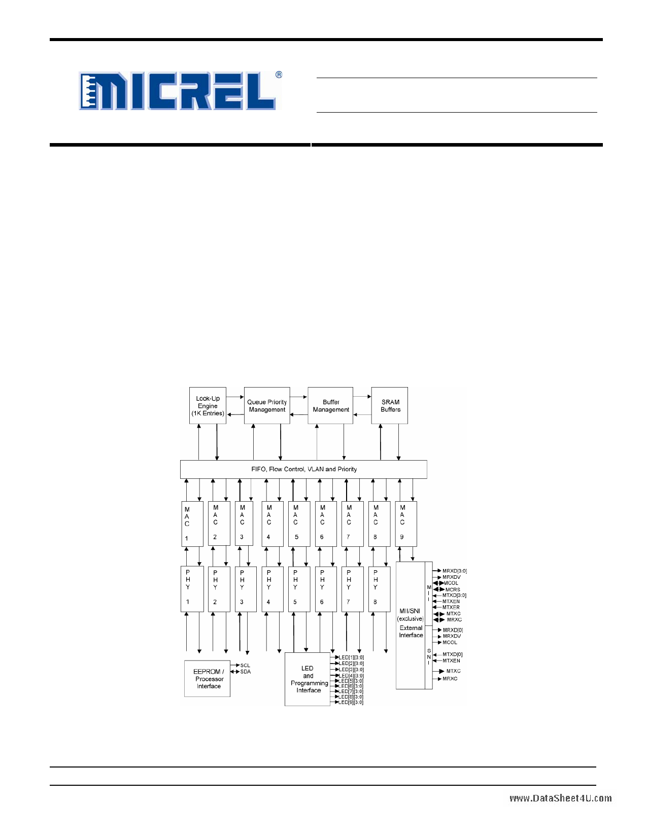
KS8999
Integrated 9-Port 10/100 Switch with
PHY and Frame Buffer
Rev 1.14
General Description
The KS8999 contains eight 10/100 physical layer
transceivers, nine MAC (Media Access Control) units
with an integrated layer 2 switch. The device runs in two
modes. The first mode is an eight port integrated switch
and the second is as a nine port switch with the ninth
port available through an MII (Media Independent
Interface). Useful configurations include a stand alone
eight port switch as well as a eight port switch with a
routing element connected to the extra MII port. The
additional port is also useful for a public network
interfacing. The KS8999 is designed to reside in an
unmanaged design not requiring processor intervention.
This is achieved through I/O strapping or EEPROM
programming at system reset time. On the media side,
the KS8999 supports 10BaseT, 100BaseTX and
100BaseFX as specified by the IEEE 802.3 committee.
Physical signal transmission and reception are
enhanced through use of analog circuitry that makes the
design more efficient and allows for lower power
consumption and smaller chip die size.
Data sheets and support documentation can be found
on Micrel’s web site at www.micrel.com.
Functional Diagram
www.DataSheet4U.com
Micrel Inc. • 2180 Fortune Drive • San Jose, CA 95131 • USA • tel +1 (408) 944-0800 • fax + 1 (408) 474-1000 • http://www.micrel.com
January 2005
KS8999
1 page 
Micrel, Inc.
KS8999
EEPROM Memory Map..................................................................................................................................................29
General Control Register ..........................................................................................................................................29
Priority Classification Control –802.1p tag field ........................................................................................................29
Port 1 Control Register .............................................................................................................................................29
Port 2 Control Register .............................................................................................................................................30
Port 3 Control Register .............................................................................................................................................30
Port 4 Control Register .............................................................................................................................................30
Port 5 Control Register .............................................................................................................................................31
Port 6 Control Register .............................................................................................................................................31
Port 7 Control Register .............................................................................................................................................31
Port 8 Control Register .............................................................................................................................................32
Port 9 Control Register .............................................................................................................................................32
Port 1 VLAN Mask Register......................................................................................................................................32
Port 2 VLAN Mask Register......................................................................................................................................33
Port 3 VLAN Mask Register......................................................................................................................................33
Port 4 VLAN Mask Register......................................................................................................................................34
Port 5 VLAN Mask Register......................................................................................................................................34
Port 6 VLAN Mask Register......................................................................................................................................35
Port 7 VLAN Mask Register......................................................................................................................................35
Port 8 VLAN Mask Register......................................................................................................................................36
Port 9 VLAN Mask Register......................................................................................................................................36
Port 1 VLAN Tag Insertion Value Registers .............................................................................................................36
Port 2 VLAN Tag Insertion Value Registers .............................................................................................................37
Port 3 VLAN Tag Insertion Value Registers .............................................................................................................37
Port 4 VLAN Tag Insertion Value Registers .............................................................................................................37
Port 5 VLAN Tag Insertion Value Registers .............................................................................................................37
Port 6 VLAN Tag Insertion Value Registers .............................................................................................................37
Port 7 VLAN Tag Insertion Value Registers .............................................................................................................37
Port 8 VLAN Tag Insertion Value Registers .............................................................................................................37
Port 9 VLAN Tag Insertion Value Registers .............................................................................................................38
Diff Serv Code Point Registers .................................................................................................................................38
Station MAC Address Registers (all ports –MAC control frames only) ....................................................................38
Absolute Maximum Ratings .........................................................................................................................................39
Operating Ratings .........................................................................................................................................................39
Electrical Characteristics .............................................................................................................................................39
Timing Diagrams ...........................................................................................................................................................41
Reference Circuits.........................................................................................................................................................47
Reset Reference Circuit................................................................................................................................................47
4B/5B Coding.................................................................................................................................................................49
MLT3 Coding..................................................................................................................................................................50
MAC Frame ....................................................................................................................................................................50
wwwS.DelaetcaStihoeneto4Uf .Icsoomlation Transformers............................................................................................................................51
Selection of Reference Oscillator/Crystal ..................................................................................................................51
Package Information .....................................................................................................................................................52
January 2005
5 KS8999
5 Page 
Micrel, Inc.
Pin Number Pin Name
117 LED[2][1]
118 LED[2][0]
119 MRXDV
120 MRXD[3]
121 MRXD[2]
122 MRXD[1]
123 MRXD[0]
124 MRXC
125 VDD-IO
126 GND
127 LED[3][3]
128 LED[3][2]
129 LED[3][1]
130 LED[3][0]
131 LED[4][3]
132 LED[4][2]
133 LED[4][1]
134 LED[4][0]
135 VDD
136 GND
137 LED[5][3]
138 LED[5][2]
139 LED[5][1]
140 LED[5][0]
141 LED[6][3]
142 LED[6][2]
143 LED[6][1]
144 LED[6][0]
145 LED[7][3]
146 LED[7][2]
147 LED[7][1]
148 VDD-IO
149 LED[7][0]
150 LED[8][3]
151 LED[8][2]
www.DataSheet4U.com
152 LED[8][1]
153 LED[8][0]
154 GND
155 GND
Type(1)
Ipu/O
Ipu/O
Opd
Opu
Opu
Opu
Opu
Ipu/O
Pwr
GND
Ipu/O
Ipu/O
Ipu/O
Ipu/O
Ipu/O
Ipu/O
Ipu/O
Ipu/O
Pwr
GND
Ipu/O
Ipu/O
Ipu/O
Ipu/O
Ipu/O
Ipu/O
Ipu/O
Ipu/O
Ipu/O
Ipu/O
Ipu/O
Pwr
Ipu/O
Ipu/O
Ipu/O
Ipu/O
Ipu/O
GND
GND
Port
2
2
9
9
9
9
9
9
3
3
3
3
4
4
4
4
5
5
5
5
6
6
6
6
7
7
7
7
8
8
8
8
Pin Function
LED indicator 1
LED indicator 0
MII receive data valid
MII receive bit 3
MII receive bit 2
MII receive bit 1
MII receive bit 0
MII receive clock
2.0V, 2.5V or 3.3V for I/O circuitry
Ground for digital circuitry
LED indicator 3
LED indicator 2
LED indicator 1
LED indicator 0
LED indicator 3
LED indicator 2
LED indicator 1
LED indicator 0
2.0V for core digital circuitry
Ground for digital circuitry
LED indicator 3
LED indicator 2
LED indicator 1
LED indicator 0
LED indicator 3
LED indicator 2
LED indicator 1
LED indicator 0
LED indicator 3
LED indicator 2
LED indicator 1
2.0V, 2.5V or 3.3V for I/O circuitry
LED indicator 0
LED indicator 3
LED indicator 2
LED indicator 1
LED indicator 0
Ground for digital circuitry
Ground for digital circuitry
January 2005
11
KS8999
KS8999
11 Page | ||
| Páginas | Total 53 Páginas | |
| PDF Descargar | [ Datasheet KS8999.PDF ] | |
Hoja de datos destacado
| Número de pieza | Descripción | Fabricantes |
| KS8993 | 3-Port 10/100 Integrated Switch | Micrel Semiconductor |
| KS8993F | Single Chip Fast Ethernet Media Converter | Micrel Semiconductor |
| KS8993FL | Single Chip Fast Ethernet Media Converter | Micrel Semiconductor |
| KS8993M | Integrated 3-Port 10/100 Managed Integrated 3-Port 10/100 Managed | Micrel Semiconductor |
| Número de pieza | Descripción | Fabricantes |
| SLA6805M | High Voltage 3 phase Motor Driver IC. |
Sanken |
| SDC1742 | 12- and 14-Bit Hybrid Synchro / Resolver-to-Digital Converters. |
Analog Devices |
|
DataSheet.es es una pagina web que funciona como un repositorio de manuales o hoja de datos de muchos de los productos más populares, |
| DataSheet.es | 2020 | Privacy Policy | Contacto | Buscar |