|
|
|
PDF KS8993FL Data sheet ( Hoja de datos )
| Número de pieza | KS8993FL | |
| Descripción | Single Chip Fast Ethernet Media Converter | |
| Fabricantes | Micrel Semiconductor | |
| Logotipo | ||
Hay una vista previa y un enlace de descarga de KS8993FL (archivo pdf) en la parte inferior de esta página. Total 30 Páginas | ||
|
No Preview Available !
KS8993F/KS8993FL
Single Chip Fast Ethernet Media
Converter with TS-1000 OAM
Revision 1.3
General Description
The Micrel KS8993F is the industry’s first single chip Fast
Ethernet Media Converter with built-in OAM functions. The
KS8993F integrates three MACs, two PHYs, OAM, frame
buffer and high performance switch into a single chip. It is
ideal for use in 100BASE-FX to 10BASE-T or 100BASE-
TX conversion in the FTTx market.
The KS8993F provides remote loop back and OAM
(Operation, Administration and Maintenance) to manage
subscriber access network from carrier center side to
terminal side.
The KS8993F supports advanced features such as rate
limiting, force flow control and link transparency.
The KS8993F with built-in Layer 2 switch capability will
filter packets and forward them to valid destination. It will
discard any unwanted frames and frames with invalid
destination.
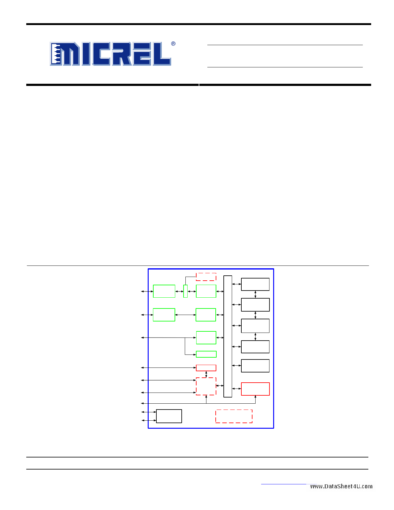
Block Diagram
The KS8993FL is the single supply version with all the
identical rich features of the KS8993F.
Features
• First single-chip 10BASE-T/100BASE-TX to
100BASE-FX media converter with TS-1000 OAM
• Integrated 3-Port 10/100 Ethernet Switch with
3 MACs and 2 PHYs
• Unique User Defined Register (UDR) feature brings
OAM to low cost/complexity nodes
• Automatic MDI/MDI-X crossover with disable and
enable option
• Non-blocking switch fabric assures fast packet
delivery by utilizing an 1K MAC Address lookup table
and a store-and-forward architecture
• Comprehensive LED indicator support for link, activity,
full/half duplex and 10/100 speed
• Full complement of MII/SNI, SPI, MIIM, SMI and I2C
interfaces
• Low Power Dissipation:< 800mW (includes PHY
transmit drivers)
www.DataSheet4U.com
Auto
MDI/MDI-X
Auto
MDI/MDI-X
MII / SNI
Interface
SPI
Interface
MIIM
Interface
SMI
Interface
I2C
Bus
P1 LED[3:0]
P2 LED[3:0]
10/100
T/TX/FX
PHY1
10/100
T/TX/FX
PHY2
To Control
Registers
O
A
10/100
MAC 1
M
10/100
MAC 2
10/100
MAC 3
SNI
SPI
Control
Registers
1K look-up
Engine
Queue
Management
Buffer
Management
Frame
Buffers
MIB
Counters
EEPROM
Interface
LED
Drivers
Strap In
Configuration Pins
KS8993F / KS8993FL
Micrel is a registered trademark of Micrel, Inc.
Micrel Inc. • 2180 Fortune Drive • San Jose, CA 95131 • USA • tel +1 (408) 944-0800 • fax + 1 (408) 474-1000 • http://www.micrel.com
June 2009
M9999-062509
[email protected] or (408) 955-1690
1 page 
Micrel, Inc.
KS8993F/FL
Register 5: Auto-Negotiation Link Partner Ability ................................................................................................................ 49
4 Register Map: Switch, MC, & PHY (8 bits registers) ..................................................................50
4.1 Global Registers................................................................................................................................................................... 51
Register 0 (0x00): Chip ID0................................................................................................................................................. 51
Register 1 (0x01): Chip ID1 / Start Switch........................................................................................................................... 51
Register 2 (0x02): Global Control 0..................................................................................................................................... 51
Register 3 (0x03): Global Control 1..................................................................................................................................... 52
Register 4 (0x04): Global Control 2..................................................................................................................................... 53
Register 5 (0x05): Global Control 3..................................................................................................................................... 53
Register 6 (0x06): Global Control 4..................................................................................................................................... 54
Register 7 (0x07): Global Control 5..................................................................................................................................... 55
Register 8 (0x08): Global Control 6..................................................................................................................................... 55
Register 9 (0x09): Global Control 7..................................................................................................................................... 55
Register 10 (0x0A): Global Control 8 .................................................................................................................................. 55
Register 11 (0x0B): Global Control 9 .................................................................................................................................. 55
Register 12 (0x0C): Reserved Register .............................................................................................................................. 56
Register 13 (0x0D): User Defined Register 1...................................................................................................................... 56
Register 14 (0x0E): User Defined Register 2 ...................................................................................................................... 57
Register 15 (0x0F): User Defined Register 3 ...................................................................................................................... 57
4.2 Port Registers ...................................................................................................................................................................... 57
Register 16 (0x10): Port 1 Control 0 ................................................................................................................................... 57
Register 17 (0x11): Port 1 Control 1 ................................................................................................................................... 58
Register 18 (0x12): Port 1 Control 2 ................................................................................................................................... 58
Register 19 (0x13): Port 1 Control 3 ................................................................................................................................... 59
Register 20 (0x14): Port 1 Control 4 ................................................................................................................................... 59
Register 21 (0x15): Port 1 Control 5 ................................................................................................................................... 60
Register 22 (0x16): Port 1 Control 6 ................................................................................................................................... 60
Register 23 (0x17): Port 1 Control 7 ................................................................................................................................... 60
Register 24 (0x18): Port 1 Control 8 ................................................................................................................................... 60
Register 25 (0x19): Port 1 Control 9 ................................................................................................................................... 60
Register 26 (0x1A): Port 1 Control 10 ................................................................................................................................. 60
Register 27 (0x1B): Port 1 Control 11 ................................................................................................................................. 61
Register 28 (0x1C): Port 1 Control 12 ................................................................................................................................. 61
Register 29 (0x1D): Port 1 Control 13 ................................................................................................................................. 62
Register 30 (0x1E): Port 1 Status 0 .................................................................................................................................... 63
Register 31 (0x1F): Port 1 Status 1..................................................................................................................................... 64
4.3 Media Converter Registers .................................................................................................................................................. 65
Register 64 (0x40): PHY Address ....................................................................................................................................... 65
Register 65 (0x41): Center Side Status .............................................................................................................................. 65
Register 66 (0x42): Center Side Command ........................................................................................................................ 66
Register 67 (0x43): PHY-SW Initialize ................................................................................................................................ 66
Register 68 (0x44): Loop Back Setup1 ............................................................................................................................... 68
Register 69 (0x45): Loop Back Setup2 ............................................................................................................................... 68
Register 70 (0x46): Loop Back Result Counter for CRC Error............................................................................................ 69
Register 71 (0x47): Loop Back Result Counter for Timeout................................................................................................ 69
Register 72 (0x48): Loop Back Result Counter for Good Packet........................................................................................ 69
Register 73 (0x49): Additional Status (Center and Terminal side) ...................................................................................... 69
Register 74 (0x4A): Remote Command 1 ........................................................................................................................... 70
Register 75 (0x4B): Remote Command 2 ........................................................................................................................... 70
Register 76 (0x4C): Remote Command 3 ........................................................................................................................... 71
Register 77 (0x4D): Valid MC Packet Transmitted Counter................................................................................................ 71
Register 78 (0x4E): Valid MC Packet Received Counter .................................................................................................... 71
Register 79 (0x4F): Shadow of 0x58h Register .................................................................................................................. 71
Register 80 (0x50): My Status 1 (Terminal and Center side) .............................................................................................. 72
Register 81 (0x51): My Status 2.......................................................................................................................................... 72
Register 82 (0x52): My Vendor Info (1) ............................................................................................................................... 73
www.DataShReeegt4isUte.cro8m3 (0x53): My Vendor Info (2) ............................................................................................................................... 73
Register 84 (0x54): My Vendor Info (3) ............................................................................................................................... 73
Register 85 (0x55): My Model Info (1)................................................................................................................................. 73
Register 86 (0x56): My Model Info (2)................................................................................................................................. 73
Register 87 (0x57): My Model Info (3)................................................................................................................................. 73
June 2009
5 M9999-062509
[email protected] or (408) 955-1690
5 Page 
Micrel, Inc.
Pin #
9
10
Pin Name
MCHS
MCCS
11 PDD#
12 ADVFC
13 P2ANEN
14 P2SPD
15 P2DPX
16 P2FFC
17 P1FST
www1.D8 ataShePet14LUC.cRoCmD
June 2009
Type
Ipd
Ipd
KS8993F/FL
Description
KS8993F operating modes, defined as below:
(MCHS, MCCS)
(0, 0)
Description
Normal 3 port switch mode (3 MAC + 2 PHY)
MC mode is disabled.
Port 1 is either Fiber or UTP.
Port 2 is UTP.
Port 3 (MII) is enabled.
(0, 1)
Center MC mode (3 MAC + 2 PHY)
MC mode is enabled.
Port 1 is Fiber and has Center MC enabled.
Port 2 is UTP.
Port 3 (MII) is enabled.
(1, 0)
Terminal MC mode (2 MAC + 2 PHY)
MC mode is enabled.
Port 1 is Fiber and has Terminal MC enabled.
Port 2 is UTP.
Port 3 (MII) is disabled.
(1, 1)
Terminal MC mode (3 MAC + 2 PHY)
MC mode is enabled.
Port 1 is Fiber and has Terminal MC enabled.
Port 2 is UTP.
Port 3 (MII) is enabled.
Ipu Power Down Detect
1 = normal operation
0 = power down detected
In Terminal MC mode (pin MCHS is ‘1’), a high to low transition to this pin
will cause port 1 (fiber) to generate and send out an “Indicate Terminal MC
Condition” OAM frame with the S0 status bit set to ‘1’.
Ipu 1= advertise the switch’s flow control capability via auto negotiation.
0 = will not advertise the switch’s flow control capability via auto negotiation.
Ipu 1 = enable auto negotiation on port 2.
0 = disable auto negotiation on port 2.
Ipd 1 = Force port 2 to 100BT if P2ANEN = 0.
0 = Force port 2 to 10BT if P2ANEN = 0.
Ipd 1 = port 2 default to full duplex mode if P2ANEN = 1 and auto negotiation
fails. Force port 2 in full duplex mode if P2ANEN = 0.
0 = port 2 default to half duplex mode if P2ANEN = 1 and auto negotiation
fails. Force port 2 in half duplex mode if P2ANEN = 0.
Ipd 1 = always enable (force) port 2 flow control feature.
0 = port 2 flow control feature enable is determined by auto negotiation
result.
Opu 1 = normal function
0 = MC in loop back mode, or MC abnormal conditions happen
Ipd In MC loop back mode,
1 = Drop OAM frames and Ethernet frames with the following errors –
11 M9999-062509
[email protected] or (408) 955-1690
11 Page | ||
| Páginas | Total 30 Páginas | |
| PDF Descargar | [ Datasheet KS8993FL.PDF ] | |
Hoja de datos destacado
| Número de pieza | Descripción | Fabricantes |
| KS8993F | Single Chip Fast Ethernet Media Converter | Micrel Semiconductor |
| KS8993FL | Single Chip Fast Ethernet Media Converter | Micrel Semiconductor |
| Número de pieza | Descripción | Fabricantes |
| SLA6805M | High Voltage 3 phase Motor Driver IC. |
Sanken |
| SDC1742 | 12- and 14-Bit Hybrid Synchro / Resolver-to-Digital Converters. |
Analog Devices |
|
DataSheet.es es una pagina web que funciona como un repositorio de manuales o hoja de datos de muchos de los productos más populares, |
| DataSheet.es | 2020 | Privacy Policy | Contacto | Buscar |