|
|
PDF K4X51163PG-FGC8 Data sheet ( Hoja de datos )
| Número de pieza | K4X51163PG-FGC8 | |
| Descripción | 32Mx16 Mobile DDR SDRAM | |
| Fabricantes | Samsung Electronics | |
| Logotipo |  |
|
Hay una vista previa y un enlace de descarga de K4X51163PG-FGC8 (archivo pdf) en la parte inferior de esta página. Total 23 Páginas | ||
|
No Preview Available !
K4X51163PG - FGC6(7)(8)
Final
Mobile DDR SDRAM
32Mx16 Mobile DDR SDRAM
(VDD/VDDQ 1.8V/1.8V)
www.DataSheet4U.com
- 1 - Revision 1.0
May 2008
1 page 
K4X51163PG - FGC6(7)(8)
5.0 FUNCTIONAL BLOCK DIAGRAM
Final
Mobile DDR SDRAM
CK, CK
ADD
CK, CK
Bank Select
16
Data Input Register
Serial to parallel
LWE
LDM
32
4Mx32
4Mx32
4Mx32
4Mx32
32 16
X16
DQi
Column Decoder
Latency & Burst Length
LCKE
LRAS LCBR LWE
LCAS
Programming Register
LWCBR
LDM
Timing Register
DM Input Register
Data Strobe
CK, CK CKE CS RAS CAS WE
DM
www.DataSheet4U.com
- 5 - Revision 1.0
May 2008
5 Page 
K4X51163PG - FGC6(7)(8)
Final
Mobile DDR SDRAM
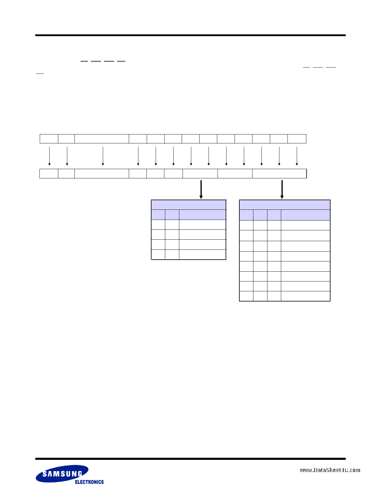
9.2 Extended Mode Register Set(EMRS)
The extended mode register is designed to support for the desired operating modes of DDR SDRAM. The extended mode register is written
by asserting low on CS, RAS, CAS, WE and high on BA1 ,low on BA0(The Mobile DDR SDRAM should be in all bank precharge with CKE
already high prior to writing into the extended mode register). The state of address pins A0 ~ A12 in the same cycle as CS, RAS, CAS and
WE going low is written in the extended mode register. Two clock cycles are required to complete the write operation in the extended mode
register. Even if the power-up sequence is finished and some read or write operations is executed afterward, the mode register contents can
be changed with the same command and two clock cycles. But this command must be issued only when all banks are in the idle state. A0 - A2
are used for partial array self refresh and A5 - A6 are used for driver strength control. "High" on BA1 and"Low" on BA0 are used for EMRS.
All the other address pins except A0,A1,A2,A5,A6, BA1, BA0 must be set to low for proper EMRS operation. Refer to the table for specific
codes.
BA1 BA0
A12 ~ A10/AP
Figure 3. Extended Mode Register Set
A9 A8 A7 A6 A5 A4 A3 A2 A1 A0 Address Bus
10
RFU1)
0 00
DS
RFU1)
PASR
Mode Register
A6 A5
00
01
10
11
DS
Driver Strength
Full
1/2
1/4
1/8
NOTE :
1) RFU(Reserved for future use) should stay "0" during EMRS cycle
PASR
A2 A1 A0 Refreshed Area
000
Full Array
001
1/2 Array
010
1/4 Array
011
Reserved
100
Reserved
101
Reserved
110
Reserved
111
Reserved
www.DataSheet4U.com
- 11 -
Revision 1.0
May 2008
11 Page | ||
| Páginas | Total 23 Páginas | |
| PDF Descargar | [ Datasheet K4X51163PG-FGC8.PDF ] | |
Hoja de datos destacado
| Número de pieza | Descripción | Fabricantes |
| K4X51163PG-FGC6 | 32Mx16 Mobile DDR SDRAM | Samsung Electronics |
| K4X51163PG-FGC7 | 32Mx16 Mobile DDR SDRAM | Samsung Electronics |
| K4X51163PG-FGC8 | 32Mx16 Mobile DDR SDRAM | Samsung Electronics |
| Número de pieza | Descripción | Fabricantes |
| SLA6805M | High Voltage 3 phase Motor Driver IC. |
Sanken |
| SDC1742 | 12- and 14-Bit Hybrid Synchro / Resolver-to-Digital Converters. |
Analog Devices |
|
DataSheet.es es una pagina web que funciona como un repositorio de manuales o hoja de datos de muchos de los productos más populares, |
| DataSheet.es | 2020 | Privacy Policy | Contacto | Buscar |
