|
|
PDF ZL6105 Data sheet ( Hoja de datos )
| Número de pieza | ZL6105 | |
| Descripción | Digital DC/DC Controller | |
| Fabricantes | Intersil Corporation | |
| Logotipo |  |
|
Hay una vista previa y un enlace de descarga de ZL6105 (archivo pdf) en la parte inferior de esta página. Total 30 Páginas | ||
|
No Preview Available !
Digital DC/DC Controller with Drivers and Auto
Compensation
ZL6105
The ZL6105 is a digital power controller with integrated
MOSFET drivers. Auto compensation eliminates the need for
manual compensation design work. Adaptive performance
optimization algorithms improve power conversion efficiency.
Zilker Labs Digital-DC™ technology enables a blend of power
conversion performance and power management features.
The ZL6105 is designed to be a flexible building block for DC
power and can be easily adapted to designs ranging from a
single-phase power supply operating from a 3.3V to a
multiphase current sharing supply operating from a 12V input.
The ZL6105 eliminates the need for complicated power supply
managers as well as numerous external discrete components.
The ZL6105 uses the I2C/SMBus™ with PMBus™ protocol for
communication with a host controller and the Digital-DC bus
for communication between Zilker Labs devices.
The ZL6105 is pin for pin compatible with the ZL2008. The
POLA VOUT table and compensation table have been removed.
A new single resistor VOUT table and the Auto Compensation
feature have been added.
Related Literature
• AN2032, “NLR Configuration for DDC Products”
• AN2033, “Zilker Labs PMBus Command Set - DDC Products”
• AN2034, “Configuring Current Sharing on the ZL2004 and
ZL2006”
• AN2035, “Compensation Using CompZL™”
Features
Power Conversion
• Efficient Synchronous Buck Controller
• Auto Compensating PID Filter
• Adaptive Light Load Efficiency Optimization
• 3V to 14V Input Range
• 0.54V to 5.5V Output Range (with margin)
• ±1% Output Voltage Accuracy
• Internal 3A MOSFET Drivers
• Fast Load Transient Response
• Current Sharing and Phase Interleaving
• Snapshot™ Parameter Capture
• Pb-Free (RoHs Compliant)
Power Management
• Digital Soft-start/stop
• Power-Good/Enable
• Voltage Tracking, Sequencing and Margining
• Voltage, Current and Temperature Monitoring
• I2C/SMBus Interface, PMBus Compatible
• Output Voltage and Current Protection
• Internal Non-volatile Memory (NVM)
Applications
• Servers/Storage Equipment
• Telecom/Datacom Equipment
• Power Supply Modules
EN PG PH_EN FC ILIM CFG UVLO V25 VR VDD
V
SS
VTRK
MGN
SYNC
DDC
SCL
SDA
SALRT
POWER
MANAGEMENT
NON-
VOLATILE
MEMORY
I2 C
PWM
CONTROLLER
MONITOR
ADC
LDO
DRIVER
CURRENT
SENSE
TEMP
SENSOR
BST
GH
SW
GL
VSEN+
VSEN-
ISENA
ISENB
SA
XTEMP
PGND SGND DGND
FIGURE 1. BLOCK DIAGRAM
100
VOUT = 3.3V
95 VOUT = 1.5V
90
85
80
75
70
65
60
55
VIN = 12V
fSW = 400kHz
Circuit of Figure
34
50
02 4 6 8
10 12 14 16 18 20
Load Current (A)
FIGURE 2. EFFICIENCY vs LOAD CURRENT
December 19, 2013
FN6906.5
1
CAUTION: These devices are sensitive to electrostatic discharge; follow proper IC Handling Procedures.
1-888-INTERSIL or 1-888-468-3774 |Copyright Intersil Americas Inc. 2011-2013. All Rights Reserved
Intersil (and design) is a trademark owned by Intersil Corporation or one of its subsidiaries.
All other trademarks mentioned are the property of their respective owners.
1 page 
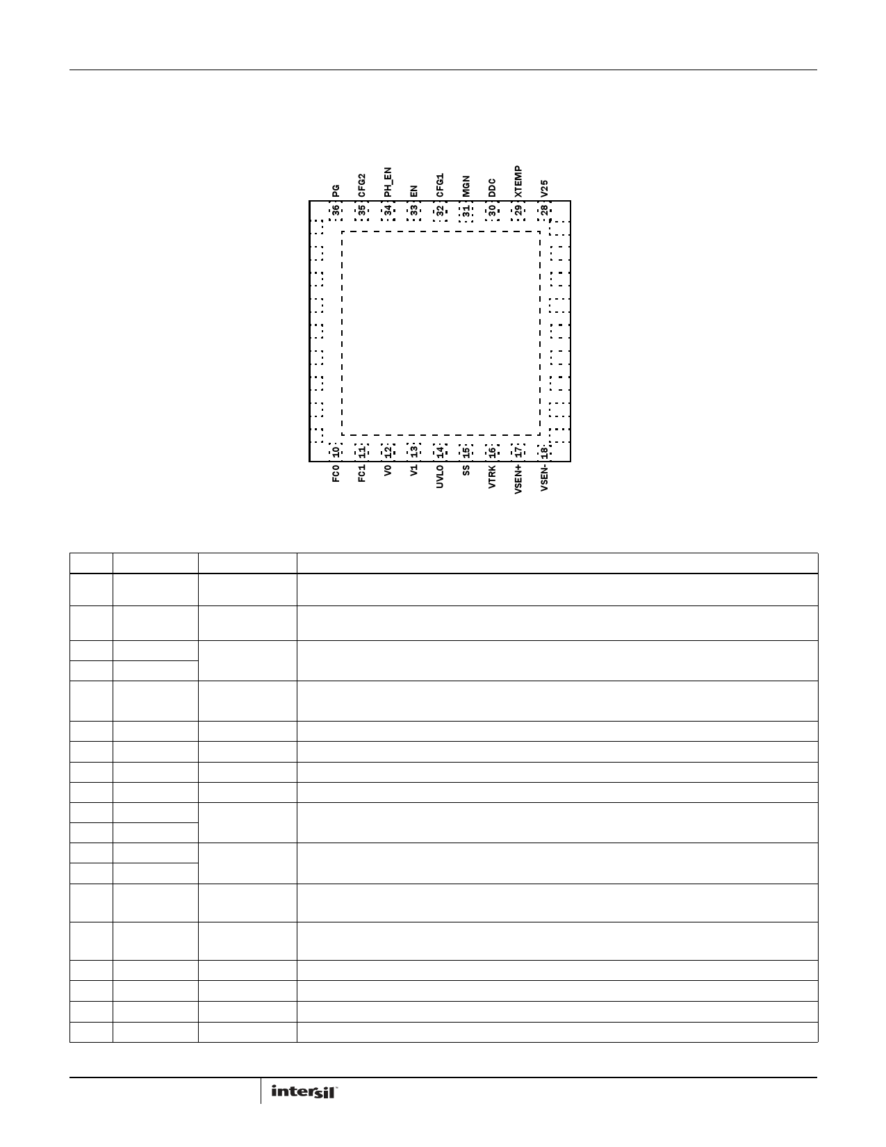
Pin Configuration
ZL6105
ZL6105
(36 LD QFN)
TOP VIEW
DGND 1
SYNC 2
SA0 3
SA1 4
ILIM 5
CFG0 6
SCL 7
SDA 8
SALRT 9
EXPOSED PADDLE*
27 VDD
26 BST
25 GH
24 SW
23 PGND
22 GL
21 VR
20 ISENA
19 ISENB
Pin Descriptions
*CONNECT TO SGND
PIN LABEL
1 DGND
TYPE (Note 1)
DESCRIPTION
PWR
Digital ground. Common return for digital signals. Connect to low impedance ground plane.
2
SYNC
I/O,M (Note 2) Clock synchronization input. Used to set switching frequency of internal clock or for synchronization to
external frequency reference.
3 SA0
4 SA1
I, M Serial address select pins. Used to assign unique SMBus address to each IC or to enable certain
management features.
5 ILIM
I, M Current limit select. Sets the overcurrent threshold voltage for ISENA and ISENB.
6 CFG0
7 SCL
8 SDA
9 SALRT
10 FC0
11 FC1
12 V0
13 V1
14 UVLO
15 SS
16 VTRK
17 VSEN+
18 VSEN-
19 ISENB
I, M Configuration pin. Used to setup current sharing and non-linear response.
I/O Serial clock. Connect to external host and/or to other ZL devices.
I/O Serial data. Connect to external host and/or to other ZL devices.
O Serial alert. Connect to external host if desired.
I Loop compensation configuration pins.
I Output voltage selection pins. Used to set VOUT set-point and VOUT max.
I, M Undervoltage lockout selection. Sets the minimum value for VDD voltage to enable VOUT.
I, M Soft start pin. Sets the output voltage ramp time during turn-on and turn-off. Sets the delay from when EN
is asserted until the output voltage starts to ramp.
I Tracking sense input. Used to track an external voltage source.
I Output voltage feedback. Connect to output regulation point.
I Output voltage feedback. Connect to load return or ground regulation point.
I Differential voltage input for current limit.
5 FN6906.5
December 19, 2013
5 Page 
ZL6105
Boost Circuit” on page 12 for more details.
In general, the size of components L1 and COUT as well as the
overall efficiency of the circuit are inversely proportional to the
switching frequency, fSW. Therefore, the highest efficiency circuit
may be realized by switching the MOSFETs at the lowest possible
frequency; however, this will result in the largest component size.
Conversely, the smallest possible footprint may be realized by
switching at the fastest possible frequency but this gives a
somewhat lower efficiency. Each user should determine the
optimal combination of size and efficiency when determining the
switching frequency for each application.
The block diagram for the ZL6105 is illustrated in Figure 4. In this
circuit, the target output voltage is regulated by connecting the
differential VSEN pins directly to the output regulation point. The
VSEN signal is then compared to a reference voltage that has
been set to the desired output voltage level by the user. The error
signal derived from this comparison is converted to a digital
value with a low-resolution, analog to digital (A/D) converter. The
digital signal is applied to an adjustable digital compensation
filter, and the compensated signal is used to derive the
appropriate PWM duty cycle for driving the external MOSFETs in a
way that produces the desired output.
The ZL6105 has several features to improve the power
conversion efficiency. A non-linear response (NLR) loop improves
the response time and reduces the output deviation as a result of
a load transient. The ZL6105 monitors the power converter’s
operating conditions and continuously adjusts the turn-on and
turn-off timing of the high-side and low-side MOSFETs to optimize
the overall efficiency of the power supply. Adaptive performance
optimization algorithms such as dead-time control, diode
emulation, and frequency control are available to provide greater
efficiency improvement.
Power Management Overview
The ZL6105 incorporates a wide range of configurable power
management features that are simple to implement with no
external components. Additionally, the ZL6105 includes circuit
protection features that continuously safeguard the device and
load from damage due to unexpected system faults. The ZL6105
can continuously monitor input voltage, output voltage/current,
internal temperature, and the temperature of an external
thermal diode. A Power-Good output signal is also included to
enable power-on reset functionality for an external processor.
All power management functions can be configured using either
pin configuration techniques (see Figure 8) or via the I2C/SMBus
interface. Monitoring parameters can also be pre-configured to
provide alerts for specific conditions. See Application Note
AN2033 for more details on SMBus monitoring.
Multi-mode Pins
In order to simplify circuit design, the ZL6105 incorporates patented
multi-mode pins that allow the user to easily configure many
aspects of the device with no programming. Most power
management features can be configured using these pins. The
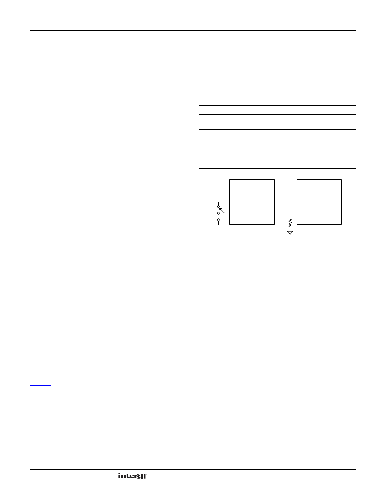
multi-mode pins can respond to four different connections as shown
in Table 1. These pins are sampled when power is applied or by
issuing a PMBus Restore command (see Application Note AN2033).
PIN-STRAP SETTINGS
This is the simplest implementation method, as no external
components are required. Using this method, each pin can take
on one of three possible states: LOW, OPEN, or HIGH. These pins
can be connected to the V25 pin for logic HIGH settings as this
pin provides a regulated voltage higher than 2V. Using a single
pin, one of three settings can be selected. Using two pins, one of
nine settings can be selected.
TABLE 1. MULTI-MODE PIN CONFIGURATION
PIN TIED TO
VALUE
LOW
(Logic LOW)
< 0.8 VDC
OPEN
(N/C)
No connection
HIGH
(Logic HIGH)
> 2.0 VDC
Resistor to SGND
Set by resistor value
Logic
ZLhigh
ZL
Open
Multi- mode Pin
Multi- mode Pin
RSET
Logic
low
Pin-strap
Settings
Resistor
Settings
FIGURE 7. PIN-STRAP AND RESISTOR SETTING EXAMPLES
RESISTOR SETTINGS
This method allows a greater range of adjustability when connecting
a finite value resistor (in a specified range) between the multi-mode
pin and SGND. Standard 1% resistor values are used, and only every
fourth E96 resistor value is used so the device can reliably recognize
the value of resistance connected to the pin while eliminating the
error associated with the resistor accuracy. Up to 31 unique
selections are available using a single resistor.
I2C/SMBUS METHOD
Almost any ZL6105 function can be configured via the I2C/SMBus
interface using standard PMBus commands. Additionally, any value
that has been configured using the pin-strap or resistor setting
methods can also be re-configured and/or verified via the
I2C/SMBus. See Application Note AN2033 for more details.
The SMBus device address and VOUT_MAX are the only
parameters that must be set by external pins. All other device
parameters can be set via the I2C/SMBus. The device address is
set using the SA0 and SA1 pins. VOUT_MAX is determined as
10% greater than the voltage set by the V0 and V1 pins.
11 FN6906.5
December 19, 2013
11 Page | ||
| Páginas | Total 30 Páginas | |
| PDF Descargar | [ Datasheet ZL6105.PDF ] | |
Hoja de datos destacado
| Número de pieza | Descripción | Fabricantes |
| ZL6100 | Adaptive Digital DC/DC Controller | Intersil Corporation |
| ZL6105 | Digital DC/DC Controller | Intersil Corporation |
| Número de pieza | Descripción | Fabricantes |
| SLA6805M | High Voltage 3 phase Motor Driver IC. |
Sanken |
| SDC1742 | 12- and 14-Bit Hybrid Synchro / Resolver-to-Digital Converters. |
Analog Devices |
|
DataSheet.es es una pagina web que funciona como un repositorio de manuales o hoja de datos de muchos de los productos más populares, |
| DataSheet.es | 2020 | Privacy Policy | Contacto | Buscar |
