|
|
|
PDF DG884 Data sheet ( Hoja de datos )
| Número de pieza | DG884 | |
| Descripción | 8 x 4 Wideband Video Crosspoint Array | |
| Fabricantes | Vishay Siliconix | |
| Logotipo | ||
Hay una vista previa y un enlace de descarga de DG884 (archivo pdf) en la parte inferior de esta página. Total 14 Páginas | ||
|
No Preview Available !
DG884
Vishay Siliconix
8 x 4 Wideband Video Crosspoint Array
FEATURES
D Routes Any Input to Any Output
D Wide Bandwidth: 300 MHz
D Low Crosstalk: −85 dB @ 5 MHz
D Double Buffered TTL-Compatible
Latches with Readback
D Low rDS(on): 45 W
D Optional Negative Supply
BENEFITS
D Reduced Board Space
D Improved System Bandwidth
D Improved Channel Off-Isolation
D Simplified Logic Interfacing
D Allows Bipolar Signal Swings
D Reduced Insertion Loss
D High Reliability
APPLICATIONS
D Wideband Signal Routing and
Multiplexing
D High-End Video Systems
D NTSC, PAL, SECAM Switchers
D Digital Video Routing
D ATE Systems
DESCRIPTION
The DG884 contains a matrix of 32 T-switches configured in
an 8 4 crosspoint array. Any of the IN/OUT pins may be
used as an input or output. Any of the IN pins may be switched
to any or simultaneously to all OUT pins.
The DG884 is built on a proprietary D/CMOS process that
combines low capacitance switching DMOS FETs with low
power CMOS control logic and drivers. The ground lines
between adjacent signal input pins help to reduce crosstalk.
The low on-resistance and low on-capacitance of the DG884
make it ideal for video and wideband signal routing.
Control data is loaded individually into four Next Event latches.
When all Next Event latches have been programmed, data is
transferred into the Current Event latches via a SALVO
command. Current Event latch data readback is available to
poll array status.
Output disable capabilities make it possible to parallel multiple
DG884s to form larger switch arrays. DIS outputs provide
control signals used to place external buffers in a power saving
mode.
For additional information see applications note AN504
(FaxBack document number 70610).
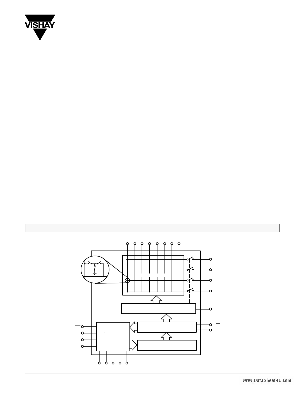
FUNCTIONAL BLOCK DIAGRAM
IN1 IN2 IN3 IN4 IN5 IN6 IN7 IN8
8 4 Switch Matrix
www.DataSheet4U.com
WR
CS
B1
B0
Decode Logic, Switch Drivers
I/O Control
Logic
Current Event Latches
Next Event Latches
OUT1
OUT2
OUT3
OUT4
4 Disable Outputs
RS
SALVO
Document Number: 70071
S-52433—Rev. G, 20-Dec-04
I/O A3 A2 A1 A0
www.vishay.com
1
1 page 
DG884
Vishay Siliconix
SPECIFICATIONSa
Parameter
Symbol
Test Conditions
Unless Specified
V+ = 15 V, V− = −3 V
VL = 5 V, RS = 2.0 V
SALVO, CS, WR, I/O = 0.8 V
A Suffix
−55 to 125_C
D Suffix
−40 to 85_C
Tempb Typc Mind Maxd Mind Maxd Unit
Power Supplies
Positive Supply Current
I+
Negative Supply Current
Digital GND Supply Current
Logic Supply Current
Functional Operating Supply Volt-
age Rangee
I−
IDG
IL
V+ to V−
V− to GND
V+ to GND
All Inputs At GND or 2 V
RS = 2 V
See Operating Voltage Range
(Typical Characteristics)
page 6
Room
1.5
3
3
Full 6 6
Room −1.5
−3
mA
−3
Full −5
−5
Full −275 −750
−750
Full 200
500
500 mA
Full 13 20 13 20
Full
−5.5 0 −5.5 0
V
Full 10 20 10 20
Minimum Input Timing Requirements
Address Write Time
Minimum WR Pulse Width
Write Address Time
Chip Select Write Time
Write Chip Select Time
Minimum SALVO
Pulse Width
tAW
tWP
tWA
tCW
tWC
tSP
Full 20 50
Full 50 100
Full −10 10
Full 50 100
Full 25 75
Full 50 100
50
100
10
100
75
100
SALVO Write Time
Write SALVO Time
Input Output Time
Address Output Time
Chip Select Output Time
Chip Select Address Time
Reset to SALVO
I/O Address Input Time
tSW
tWS
tIO
tAO
tCO
tCA
tRS
tIA
See Figure 1
Full −10 10
Room
20
Room 150 200
Room 150 200
Room 150 200
Room
60
Full 50
Room
50
10
50
200
200
200
100
50
Notes:
a. Refer to PROCESS OPTION FLOWCHART.
b. Room = 25_C, Full = as determined by the operating temperature suffix.
c. Typical values are for DESIGN AID ONLY, not guaranteed nor subject to production testing.
d. The algebraic convention whereby the most negative value is a minimum and the most positive a maximum, is used in this data sheet.
e. Guaranteed by design, not subject to production test.
ns
www.DataSheet4U.com
Document Number: 70071
S-52433—Rev. G, 20-Dec-04
www.vishay.com
5
5 Page 
DG884
Vishay Siliconix
DEVICE DESCRIPTION
Readback
The I/O facility enables the user to write data to the Next Event
latches or to read the contents of the Current Event latches.
This feature permits the central controller to periodically
monitor the state of the matrix. If a power loss to the controller
occurs, the readback feature helps the matrix to recover
rapidly. It also offers a means to perform PC board diagnostics
both in production and in system operation.
8 Analog Inputs
I/O
RS
A0
A1
A2
A3
B0
B1
CS
WR
SALVO
EN
4 Data
/ Buffers
EN
4
Q0 − Q3
4
/
7
/
Decoders/
Drivers
9
/
Mux 3 Decoder
DIS3
Open Drain
Output
One of Four Blocks of Logic/Latches Shown
FIGURE 12. Control Circuitry
Mux 1
8
OUT1
Mux 2
8
OUT2
8 T-Switches
1 Series Switch
8
OUT3
Mux 4
OUT4
APPLICATIONS
Two—Si584
Quad Unity-Gain Buffers
IN1
75 W
IN2
x1
x1
www.DataSheet4U.com
IN8
x1
WR SALVO
DG884
RS
DIS1
DIS2
DIS3
DIS4
RESET
B0 B1 A0 A1 A2 A3
CLC410
75 W
x2
x2
x2
x2
OUT1
OUT2
OUT3
OUT4
Note: DIS outputs are used to
power down the Si582 amplifiers.
FIGURE 13. Fully Buffered 8 X 4 Crosspoint
Document Number: 70071
S-52433—Rev. G, 20-Dec-04
www.vishay.com
11
11 Page | ||
| Páginas | Total 14 Páginas | |
| PDF Descargar | [ Datasheet DG884.PDF ] | |
Hoja de datos destacado
| Número de pieza | Descripción | Fabricantes |
| DG884 | 8 x 4 Wideband Video Crosspoint Array | Vishay Siliconix |
| Número de pieza | Descripción | Fabricantes |
| SLA6805M | High Voltage 3 phase Motor Driver IC. |
Sanken |
| SDC1742 | 12- and 14-Bit Hybrid Synchro / Resolver-to-Digital Converters. |
Analog Devices |
|
DataSheet.es es una pagina web que funciona como un repositorio de manuales o hoja de datos de muchos de los productos más populares, |
| DataSheet.es | 2020 | Privacy Policy | Contacto | Buscar |