|
|
|
PDF ICS844246I Data sheet ( Hoja de datos )
| Número de pieza | ICS844246I | |
| Descripción | FEMTOCLOCKS CRYSTAL-TO-LVDS FREQUENCY SYNTHESIZER W/INTEGRATED FANOUT BUFFER | |
| Fabricantes | Integrated Device Technology | |
| Logotipo | ||
Hay una vista previa y un enlace de descarga de ICS844246I (archivo pdf) en la parte inferior de esta página. Total 16 Páginas | ||
|
No Preview Available !
PRELIMINARY
FEMTOCLOCKS™ CRYSTAL-TO-LVDS
FREQUENCY SYNTHESIZER W/INTEGRATED FANOUT BUFFER
ICS844246I
GENERAL DESCRIPTION
ICS
HiPerClockS™
The ICS844246I is a Cr ystal-to-LVDS Clock
Synthesizer/Fanout Buffer designed for Fibre
Channel and Gigabit Ethernet applications and is
a member of the HiperClockS™ family of High
Performance Clock Solutions from IDT. The output
frequency can be set using the frequency select pins and a
25MHz crystal for Ethernet frequencies, or a 26.5625MHz
crystal for a Fibre Channel. The low phase noise character-
istics of the ICS844246I make it an ideal clock for these
demanding applications.
SELECT FUNCTION TABLE
Inputs
FB_SEL N_SEL1 N_SEL0
00 0
00
1
0 10
011
10
0
10
1
110
11 1
M Divide
20
20
20
20
24
24
24
24
Function
N Divide
2
4
5
8
3
4
6
12
M/N
10
5
4
2.5
8
6
4
2
FEATURES
• Six LVDS outputs
• Crystal oscillator interface
• Output frequency range: 53.125MHz to 333.3333MHz
• Crystal input frequency range: 25MHz to 33.333MHz
• RMS phase jitter at 125MHz, using a 25MHz crystal
(1.875MHz to 20MHz): 0.39ps (typical)
• Full 3.3V or 3.3V core, 2.5V output supply mode
• -40°C to 85°C ambient operating temperature
• Available in both standard (RoHS 5) and lead-free (RoHS 6)
packages
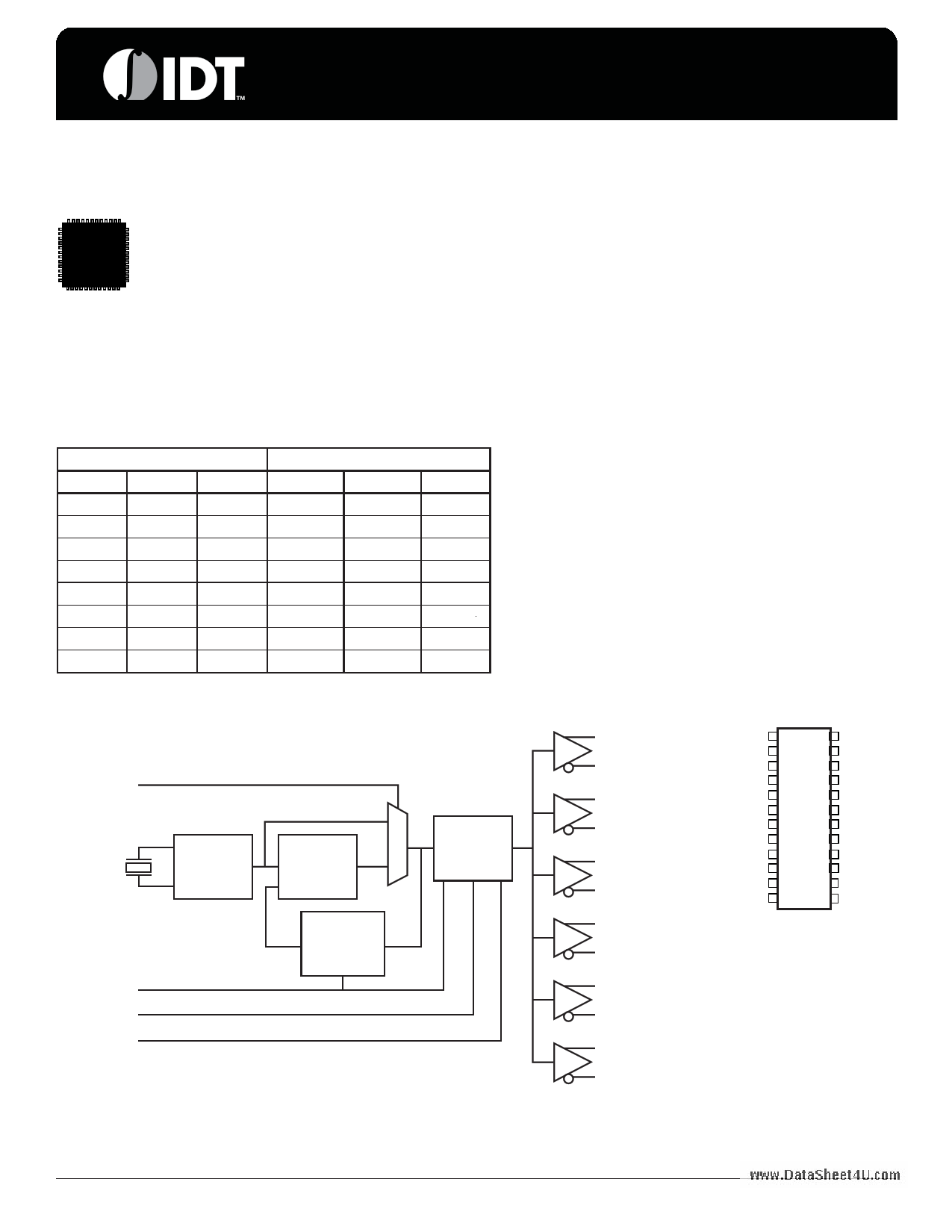
BLOCK DIAGRAM
PIN ASSIGNMENT
PLL_BYPASS Pullup
XTAL_IN
XTAL_OUT
OSC
FB_SEL Pulldown
www.DNa_taSSELh1eetP4uUllu.pcom
Pullup
N_SEL0
1
Output
PLL 0 Divider
Feedback
Divider
Q0
nQ0
Q1
nQ1
Q2
nQ2
VDDO
VDDO
nQ2
Q2
nQ1
Q1
nQ0
Q0
PLL_BYPASS
VDDA
VDD
FB_SEL
1
2
3
4
5
6
7
8
9
10
11
12
24 Q3
23 nQ3
22 Q4
21 nQ4
20 Q5
19 nQ5
18 N_SEL1
17 GND
16 GND
15 N_SEL0
14 XTAL_OUT
13 XTAL_IN
Q3 ICS844246I
nQ3 24-Lead TSSOP, E-Pad
4.40mm x 7.8mm x 0.90mm
Q4 body package
G Package
nQ4 Top View
Q5
nQ5
The Preliminary Information presented herein represents a product in pre-production. The noted characteristics are based on initial product characterization
and/or qualification. Integrated Device Technology, Incorporated (IDT) reserves the right to change any circuitry or specifications without notice.
IDT™ / ICS™ LVDS FREQUENCY SYNTHESIZER W/FANOUT BUFFER 1
ICS844246BGI REV. A NOVEMBER 14, 2007
1 page 
ICS844246I
FEMTOCLOCKS™ CRYSTAL-TO-LVDS FREQUENCY SYNTHESIZER W/INTEGRATED FANOUT BUFFER PRELIMINARY
TABLE 4D. LVDS DC CHARACTERISTICS, VDD = VDDO = 3.3V±5% TA = -40°C TO 85°C
Symbol Parameter
Test Conditions
Minimum
VOD Differential Output Voltage
Δ VOD
VOD Magnitude Change
VOS Offset Voltage
Δ VOS
VOS Magnitude Change
NOTE: Please refer to Parameter Measurement Information for output information.
Typical
387
40
1.29
50
Maximum
Units
mV
mV
V
mV
TABLE 4E. LVDS DC CHARACTERISTICS, VDD = 3.3V±5%, VDDO = 2.5V±5%, TA = -40°C TO 85°C
Symbol Parameter
Test Conditions
Minimum Typical
VOD
Δ VOD
VOS
Δ VOS
Differential Output Voltage
VOD Magnitude Change
Offset Voltage
VOS Magnitude Change
379
40
1.24
50
Maximum
Units
mV
mV
V
mV
TABLE 5. CRYSTAL CHARACTERISTICS
Parameter
Test Conditions
Mode of Oscillation
Frequency
Equivalent Series Resistance (ESR)
Shunt Capacitance
Drive Level
NOTE: Characterized using an 18pf parallel resonant crystal.
Minimum Typical Maximum
Fundamental
25 33.333
50
7
1
Units
MHz
Ω
pF
mW
www.DataSheet4U.com
IDT™ / ICS™ LVDS FREQUENCY SYNTHESIZER W/FANOUT BUFFER 5
ICS844246BGI REV. A NOVEMBER 14, 2007
5 Page 
ICS844246I
FEMTOCLOCKS™ CRYSTAL-TO-LVDS FREQUENCY SYNTHESIZER W/INTEGRATED FANOUT BUFFER PRELIMINARY
EPAD THERMAL RELEASE PATH
In order to maximize both the removal of heat from the package
and the electrical performance, a land pattern must be
incorporated on the Printed Circuit Board (PCB) within the footprint
of the package corresponding to the exposed metal pad or
exposed heat slug on the package, as shown in Figure 5. The
solderable area on the PCB, as defined by the solder mask, should
be at least the same size/shape as the exposed pad/slug area on
the package to maximize the thermal/electrical performance.
Sufficient clearance should be designed on the PCB between the
outer edges of the land pattern and the inner edges of pad pattern
for the leads to avoid any shorts.
While the land pattern on the PCB provides a means of heat
transfer and electrical grounding from the package to the board
through a solder joint, thermal vias are necessary to effectively
conduct from the surface of the PCB to the ground plane(s). The
land pattern must be connected to ground through these vias.
The vias act as “heat pipes”. The number of vias (i.e. “heat pipes”)
are application specific and dependent upon the package power
dissipation as well as electrical conductivity requirements. Thus,
thermal and electrical analysis and/or testing are recommended
to determine the minimum number needed. Maximum thermal
and electrical performance is achieved when an array of vias is
incorporated in the land pattern. It is recommended to use as
many vias connected to ground as possible. It is also
recommended that the via diameter should be 12 to 13mils (0.30
to 0.33mm) with 1oz copper via barrel plating. This is desirable to
avoid any solder wicking inside the via during the soldering process
which may result in voids in solder between the exposed pad/
slug and the thermal land. Precautions should be taken to
eliminate any solder voids between the exposed heat slug and
the land pattern. Note: These recommendations are to be used
as a guideline only. For further information, refer to the Application
Note on the Surface Mount Assembly of Amkor’s Thermally/
Electrically Enhance Leadfame Base Package, Amkor Technology.
SOLDER
PIN
EXPOSED HEAT SLUG
SOLDER PIN
SOLDER
PIN PAD
GROUND PLANE
THERMAL VIA
LAND PATTERN
(GROUND PAD)
PIN PAD
FIGURE 5. ASSEMBLY FOR EXPOSED PAD THERMAL RELEASE PATH –SIDE VIEW (DRAWING NOT TO SCALE)
www.DataSheet4U.com
IDT™ / ICS™ LVDS FREQUENCY SYNTHESIZER W/FANOUT BUFFER 11
ICS844246BGI REV. A NOVEMBER 14, 2007
11 Page | ||
| Páginas | Total 16 Páginas | |
| PDF Descargar | [ Datasheet ICS844246I.PDF ] | |
Hoja de datos destacado
| Número de pieza | Descripción | Fabricantes |
| ICS844246 | CRYSTAL-TO-LVDS FREQUENCY SYNTHESIZER W/INTEGRATED FANOUT BUFFER | ICS |
| ICS844246I | FEMTOCLOCKS CRYSTAL-TO-LVDS FREQUENCY SYNTHESIZER W/INTEGRATED FANOUT BUFFER | Integrated Device Technology |
| Número de pieza | Descripción | Fabricantes |
| SLA6805M | High Voltage 3 phase Motor Driver IC. |
Sanken |
| SDC1742 | 12- and 14-Bit Hybrid Synchro / Resolver-to-Digital Converters. |
Analog Devices |
|
DataSheet.es es una pagina web que funciona como un repositorio de manuales o hoja de datos de muchos de los productos más populares, |
| DataSheet.es | 2020 | Privacy Policy | Contacto | Buscar |