|
|
|
PDF CHM8958JPT Data sheet ( Hoja de datos )
| Número de pieza | CHM8958JPT | |
| Descripción | Dual Enhancement Mode Field Effect Transistor | |
| Fabricantes | Chenmko Enterprise | |
| Logotipo | ||
Hay una vista previa y un enlace de descarga de CHM8958JPT (archivo pdf) en la parte inferior de esta página. Total 5 Páginas | ||
|
No Preview Available !
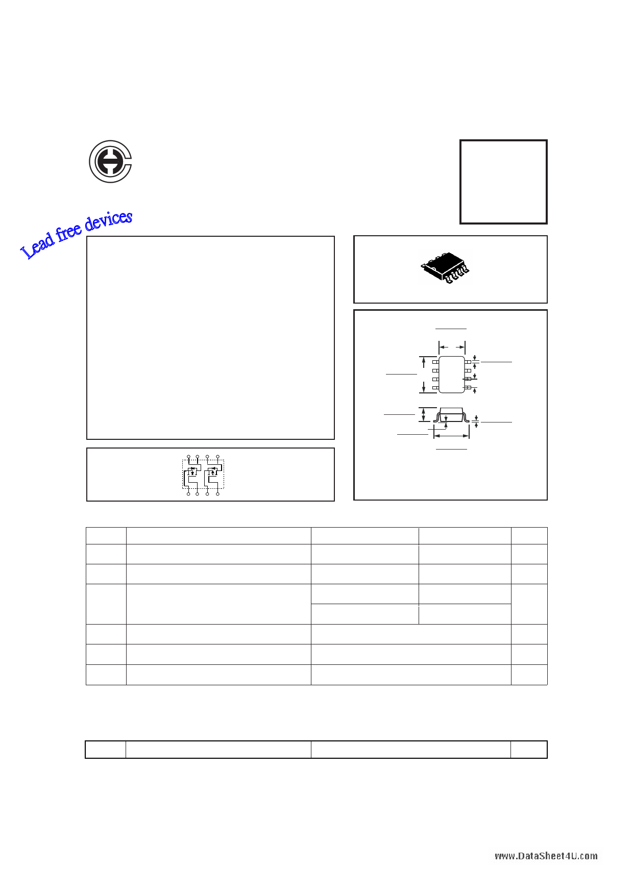
CHENMKO ENTERPRISE CO.,LTD
SURFACE MOUNT
Dual Enhancement Mode Field Effect Transistor
N-channel: VOLTAGE 30 Volts CURRENT 7 Ampere
P-channel: VOLTAGE 30 Volts CURRENT 5.2 Ampere
CHM8958JPT
APPLICATION
* Servo motor control.
* Power MOSFET gate drivers.
* Other switching applications.
FEATURE
* Small flat package. (SO-8 )
* Super high dense cell design for extremely low RDS(ON).
* Lead free product is acquired.
* High power and current handing capability.
CONSTRUCTION
* N-Channel & P-Channel Enhancement in the package
CIRCUIT
8D1 D1 D2 D25
SO-8
4.06 (0.160)
3.70 (0.146)
5.00 (0.197)
4.69 (0.185)
1
4
8
5
1.75 (0.069)
1.35 (0.053)
.25 (0.010)
.05 (0.002)
6.20 (0.244)
5.80 (0.228)
.51 (0.020)
.10 (0.012)
1.27 (0.05)BSC
.25 (0.010)
.17 (0.007)
1S1 G1 S2 G24
Dimensions in millimeters
Absolute Maximum Ratings
Symbol Parameter
VDSS
Drain-Source Voltage
VGSS
Gate-Source Voltage
TA = 25°C unless otherwise noted
N-Channel
30
±20
P-Channel
-30
±20
Maximum Drain Current - Continuous
ID
- Pulsed (Note 3)
7.0
20
-5.2
-20
PD Maximum Power Dissipation
TJ Operating Temperature Range
2000
-55 to 150
TSTG Storage Temperature Range
Note : 1. Surface Mounted on FR4 Board , t <=10sec
2. Pulse Test , Pulse width <= 300us , Duty Cycle <= 2%
3. Repetitive Rating , Pulse width linited by maximum junction temperature
4. Guaranteed by design , not subject to production trsting
Thermal characteristics
www.DataSheet4U.com
RθJA
Thermal Resistance, Junction-to-Ambient (Note 1)
-55 to 150
62.5
SO-8
Units
V
V
A
mW
°C
°C
°C/W
2006-02
1 page 
RATING CHARACTERISTIC CURVES ( CHM8958JPT )
P-Channel Typical Electrical Characteristics
Figure 1. Output Characteristics
30
VG S =- 1 0 , - 6 V V
VG S =- 5 . 0 V
24
VG S =- 4 . 5 V
18
12
6
0
0
VG S =- 4 . 0 V
VG S =- 3 . 5 V
VG S =-3 . 0 V
1.0 2.0
3.0 4.0 5.0
-VDS , DRAIN-TO-SOURCE VOLTAGE (V)
6.0
Figure 2. Transfer Characteristics
15
12
9
6
3
0
1.5
TJ=125°C
TJ=-55°C
TJ=25°C
2.0 2.5 3.0 3.5 4.0
-VGS , GATE-TO-SOURCE VOLTAGE (V)
4.5
Figure 3. Gate Charge
10
VDS=-15V
ID=-5.3A
8
6
4
2
0
03
6
9
Qg , TOTAL GATE CHARGE (nC)
Figure 4. On-Resistance Variation with
Temperature
2.2
VGS=5V
ID=10A
1.9
1.6
1.3
1.0
0.7
0.4
12
-100
-50
0
50
100 150
200
TJ , JUNCTION T EMPERATURE (°C)
Figure 5. Gate Threshold Variation with
Temperature
1.3
VDS=VGS
ID=250uA
1.2
1.1
1.0
0.9
0.8
0.7
0.6
-50
-25
0
25 50
75 100
TJ , JUNCTION T EMPERATURE (°C)
125
150
www.DataSheet4U.com
5 Page | ||
| Páginas | Total 5 Páginas | |
| PDF Descargar | [ Datasheet CHM8958JPT.PDF ] | |
Hoja de datos destacado
| Número de pieza | Descripción | Fabricantes |
| CHM8958JPT | Dual Enhancement Mode Field Effect Transistor | Chenmko Enterprise |
| Número de pieza | Descripción | Fabricantes |
| SLA6805M | High Voltage 3 phase Motor Driver IC. |
Sanken |
| SDC1742 | 12- and 14-Bit Hybrid Synchro / Resolver-to-Digital Converters. |
Analog Devices |
|
DataSheet.es es una pagina web que funciona como un repositorio de manuales o hoja de datos de muchos de los productos más populares, |
| DataSheet.es | 2020 | Privacy Policy | Contacto | Buscar |