|
|
PDF PCS3P2537A Data sheet ( Hoja de datos )
| Número de pieza | PCS3P2537A | |
| Descripción | Peak EMI Reduction IC | |
| Fabricantes | ON Semiconductor | |
| Logotipo | ||
Hay una vista previa y un enlace de descarga de PCS3P2537A (archivo pdf) en la parte inferior de esta página. Total 7 Páginas | ||
|
No Preview Available !
PCS3P2537A
Peak EMI Reduction IC
Features
• 1x Peak EMI Reduction IC
• Input Frequency: 18MHz-36MHz
• Output Frequency: 18MHz-36MHz
• Frequency Deviation @ 27MHz: -0.25%
• Modulation Rate @ 27MHz: 30.1KHz
• Supply Voltage: 3.3V ± 0.3V
• Operating current less than 8mA @ 27MHz
• Spread Spectrum Enable Control
• CMOS design
• 8L-WDFN (8L-TDFN) package
Product Description
PCS3P2537A is a 1x spread spectrum frequency
modulator designed to reduce electromagnetic
interference (EMI) at the clock source, allowing system
wide reduction of EMI of down stream clock and data
dependent signals. The device allows significant system
cost savings by reducing the number of circuit board
layers, ferrite beads and shielding and other passive
components that are traditionally required to pass EMI
regulations.
PCS3P2537A modulates the output of wa wswing.DleatPaSLhLeeint4U.com
order to “spread” the bandwidth of a synthesized clock,
and more importantly, decreases the peak amplitudes of
its harmonics. This result in significantly lower system
EMI compared to the typical narrow band signal produced
by oscillators and most frequency generators. Lowering
EMI by increasing a signal’s bandwidth is called ‘spread
spectrum clock generation.’
PCS3P2537A has a frequency range of 18MHz-36MHz,
and accepts input clock either from a Crystal or from an
external reference and locks on to it delivering a 1x
spread spectrum clock output. It has an SSON control for
enabling and disabling Spread Spectrum function.
PCS3P2537A operates with a supply voltage of 3.3V, and
is available in 8 L-WDFN package.
Application
PCS3P2537A is targeted towards PC peripheral devices
and embedded systems.
Block Diagram
VDD
SSON
CLKIN / XIN
XOUT
Crystal
Oscillator
PLL
ModOUT
GND
©2010 SCILLC. All rights reserved.
JANUARY 2010 – Rev. 1
Publication Order Number:
PCS3P2537/D
1 page 
PCS3P2537A
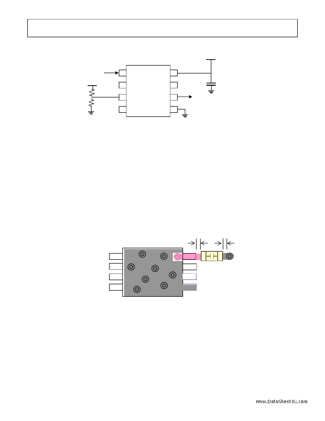
Typical Application Schematic
CLKIN / XIN
1 CLKIN / XIN
VDD 8
VDD
0Ω
0Ω
2 XOUT
3 SSON
4 NC
NC 7
ModOUT 6
GND 5
VDD
0.01uF
Note: Refer to Pin Description table for Functionality Details.
www.DataSheet4U.com
PCB Layout Recommendation
For optimum device performance, the following guidelines
are recommended.
• Dedicated VDD and GND planes.
• The device must be isolated from system power
supply noise. A 0.01µF decoupling capacitor should
be mounted on the component side of the board as
close to the VDD pin as possible. No vias should be
A typical layout is shown in the figure
CLKIN
XOUT
SSON
NC
used between the decoupling capacitor and VDD pin.
The PCB trace to VDD pin and the ground via should
be kept as short as possible. All the VDD pins should
have decoupling capacitors.
• In an optimum layout all components are on the
same side of the board, minimizing vias through
other signal layers.
As short
as possible
VDD
NC
MoGdNoDut
GND
Rev. 1 | Page 5 of 7 | www.onsemi.com
5 Page | ||
| Páginas | Total 7 Páginas | |
| PDF Descargar | [ Datasheet PCS3P2537A.PDF ] | |
Hoja de datos destacado
| Número de pieza | Descripción | Fabricantes |
| PCS3P2537A | Low Power Peak EMI Reduction IC | PulseCore Semiconductor |
| PCS3P2537A | Peak EMI Reduction IC | ON Semiconductor |
| Número de pieza | Descripción | Fabricantes |
| SLA6805M | High Voltage 3 phase Motor Driver IC. |
Sanken |
| SDC1742 | 12- and 14-Bit Hybrid Synchro / Resolver-to-Digital Converters. |
Analog Devices |
|
DataSheet.es es una pagina web que funciona como un repositorio de manuales o hoja de datos de muchos de los productos más populares, |
| DataSheet.es | 2020 | Privacy Policy | Contacto | Buscar |
