|
|
|
PDF PA7128 Data sheet ( Hoja de datos )
| Número de pieza | PA7128 | |
| Descripción | Programmable Electrically Erasable Logic Array | |
| Fabricantes | Integrated Circuit Technology | |
| Logotipo | ||
Hay una vista previa y un enlace de descarga de PA7128 (archivo pdf) en la parte inferior de esta página. Total 6 Páginas | ||
|
No Preview Available !
CPoAmInm7due1src2triai8al/l
PA7128 PEELTM Array
Programmable Electrically Erasable Logic Array
Features
s CMOS Electrically Erasable Technology
− Reprogrammable in 28-pin DIP, SOIC and PLCC
packages
− As fast as 9ns/15ns (tpdi/tpdx), 83.3MHz (fMAX)
− Industrial grade available for 4.5 to 5.5V Vcc
and -40 to +85 °C temperatures
s Versatile Logic Array Architecture
− 12 I/Os, 14 inputs, 36 registers/latches
− Up to 36 logic cell output functions
− PLA structure with true product-term sharing
− Logic functions and registers can be I/O-buried
s Ideal for Combinatorial, Synchronous and Asyn-
chronous Logic Applications
− Integration of multiple PLDs and random logic
− Buried counters, complex state-machines
− Comparitors, decoders, other wide-gate functions
s Flexible Logic Cell
− Up to 3 output functions per logic cell
− D,T and JK registers with special features
− Independent or global clocks, resets, presets, clock
polarity and output enables
− Sum-of-products logic for output enables
s Development and Programmer Support
− ICT PLACE Development Software
− Fitters for ABEL, CUPL and other software
− Programming support by ICT PDS-3 and other popu-
lar third-party programmers.
s High-Speed Commercial and Industrial Versions
General Description
The PA7128 is a member of the Programmable Electrically
Erasable Logic (PEEL™) Array family based on ICT’s
CMOS EEPROM technology. PEEL™ Arrays free design-
ers from the limitations of ordinary PLDs by providing the
architectural flexibility and speed needed for today’s pro-
grammable logic designs. The PA7128 offers a versatile
logic array architecture with 12 I/O pins, 14 input pins and
36 registers/latches (12 buried logic cells, 12 input regis-
ters/latches, 12 buried I/O registers/latches). Its logic array
implements 50 sum-of-products logic functions that share
64 product terms. The PA7128’s logic and I/O cells (LCCs,
IOCs) are extremely flexible offering up to three output
functions per cell (a total of 36 for all 12 logic cells). Cells
are configurable as D, T and JK registers with independent
or global clocks, resets, presets, clock polarity and other
special features, making the PA7128 suitable for a variety of
combinatorial, synchronous and asynchronous logic appli-
cations. The PA7128 offers pin compatibility and super-set
functionality to popular 28-pin PLDs, such as the 26V12.
Thus, designs that exceed the architectures of such
devices can be expanded upon. The PA7128 supports
speeds as fast as 9ns/15ns (tpdi/tpdx) and 83.3MHz (fMAX)
at moderate power consumption 105mA (75mA typical).
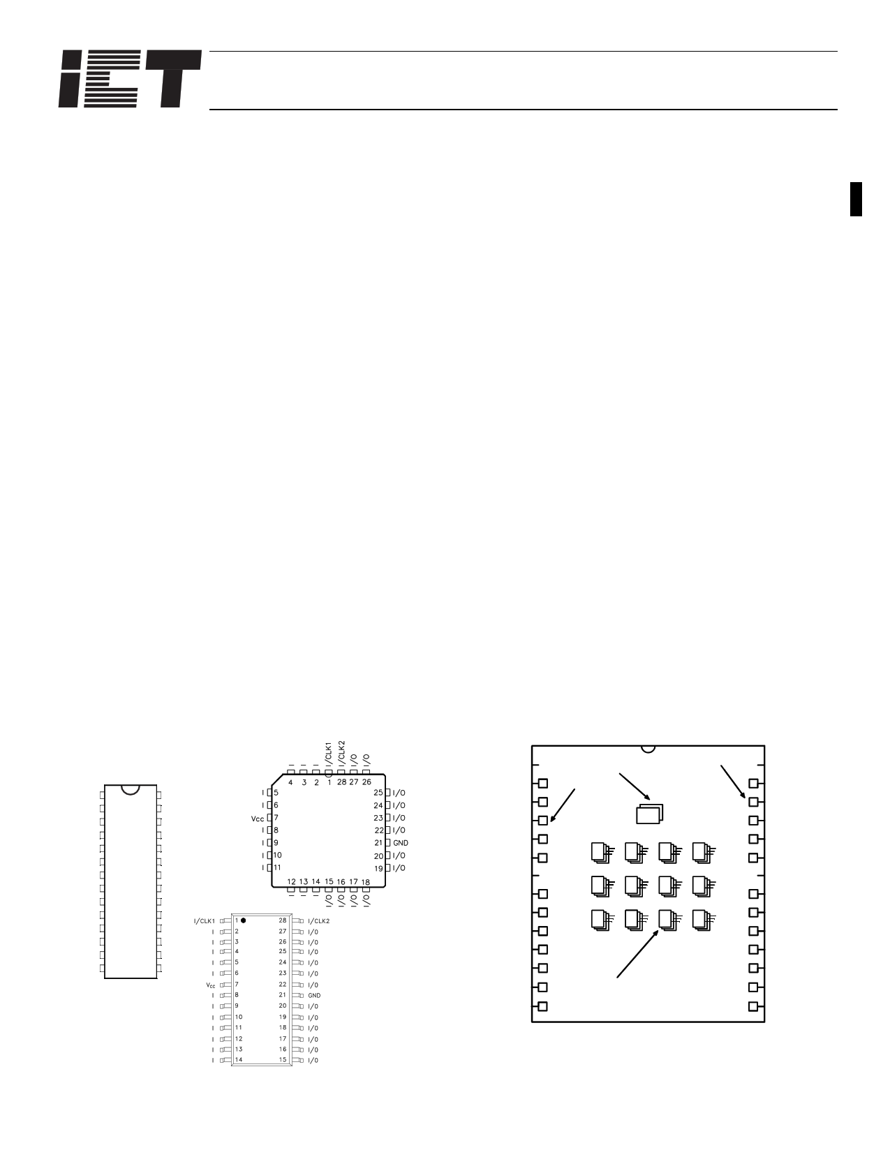
Packaging includes 28-pin DIP, SOIC and PLCC (see Fig-
ure 1). Development and programming support for the
PA7128 is provided by ICT and popular third-party develop-
ment tool manufacturers.
2
Figure 1. Pin Configuration
Figure 2. Block Diagram
1/CLK1
I
I
I
I
I
Vcc
I
I
I
I
I
I
I
1
2
3
4
5
6
7
8
9
10
11
12
13
14
28 1/CLK2
27 I/O
26 I/O
25 I/O
24 I/O
23 I/O
22 I/O
21 GND
20 I/O
19 I/O
18 I/O
17 I/O
16 I/O
15 I/O
DIP
PLCC
1/CLK
1
1
1
1
1
1
Vcc
1
1
1
1
1
1
1
Global Cells
Input Cells
Logic Control Cells
I/O Cells
1CLK2
I/O
I/O
I/O
I/O
I/O
GND
I/O
I/O
I/O
I/O
I/O
I/O
I/O
SOIC
www.DataSheet.in
1 of 6
1 page 
Sequential Timing - Waveforms and Block Diagram
PA7128
2
Notes:
1. Minimum DC input is -0.5V, however inputs may under-shoot to -2.0V for
periods less than 20ns.
2. Test points for Clock and VCC in tR, tF, tCL, tCH, and tRESET are referenced
at 10% and 90% levels.
3. I/O pins are 0V or VCC.
4. Test one output at a time for a duration of less than 1 sec.
5. Capacitances are tested on a sample basis.
6. Test conditions assume: signal transition times of 5ns or less from the
10% and 90% points, timing reference levels of 1.5V (unless otherwise
specified).
7. tOE is measured from input transition to VREF 0.1V (See test loads at
end of Section 6 for VREF value). tOD is measured from input transition to
VOH -0.1V or VOL +0.1V.
8. “System-clock” refers to pin 1 or pin 28 high speed clocks.
9. For T or JK registers in toggle (divide by 2) operation only.
10. For combinatorial and async-clock to LCC output delay.
11. ICC for a typical application: This parameter is tested with the device
programmed as a 10-bit D-type counter.
12. Test loads are specified in Section 5 of this Data Book.
13. “Async. clock” refers to the clock from the Sum term (OR gate).
14. The “LCC” term indicates that the timing parameter is applied to the
LCC register. The “IOC” term indicates that the timing parameter is
applied to the IOC register. The “LCC/IOC” term indicates that the tim-
ing parameter is applied to both the LCC and IOC registers. The “LCC/
IOC/INC” term indicates that the timing parameter is applied to the
LCC, IOC and INC registers.
15. This refers to the Sum-D gate routed to the IOC register for an addi-
tional buried register
16. The term “Input” without any reference to another term refers to an
(external) input pin.
17. The parameter tSPI indicates that the PCLK signal to the IOC register is
always slower than the data from the pin or input by the absolute value
of (tSK -tPK -tIA). This means that no set-up time for the data from the
pin or input is required, i.e. the external data and clock can be sent to
the device simultaneously. Additionally, the data from the pin must
remain stable for tHPI time, i.e. to wait for the PCLK signal to arrive at
the IOC register.
18. Typical (typ) ICC is measured at TA =25 o C, Freq = 25MHz, VCC =5V.
www.DataSheet.in
5 of 6
5 Page | ||
| Páginas | Total 6 Páginas | |
| PDF Descargar | [ Datasheet PA7128.PDF ] | |
Hoja de datos destacado
| Número de pieza | Descripción | Fabricantes |
| PA7128 | Programmable Electrically Erasable Logic Array | Integrated Circuit Technology |
| Número de pieza | Descripción | Fabricantes |
| SLA6805M | High Voltage 3 phase Motor Driver IC. |
Sanken |
| SDC1742 | 12- and 14-Bit Hybrid Synchro / Resolver-to-Digital Converters. |
Analog Devices |
|
DataSheet.es es una pagina web que funciona como un repositorio de manuales o hoja de datos de muchos de los productos más populares, |
| DataSheet.es | 2020 | Privacy Policy | Contacto | Buscar |