|
|
PDF K5L2731CAM-D770 Data sheet ( Hoja de datos )
| Número de pieza | K5L2731CAM-D770 | |
| Descripción | 128Mb NOR Flash + 32Mb UtRAM | |
| Fabricantes | Samsung Electronics | |
| Logotipo |  |
|
Hay una vista previa y un enlace de descarga de K5L2731CAM-D770 (archivo pdf) en la parte inferior de esta página. Total 30 Páginas | ||
|
No Preview Available !
K5L2731CAM-D770
Preliminary
MCP MEMORY
MCP Specification
128Mb NOR Flash + 32Mb UtRAM
INFORMATION IN THIS DOCUMENT IS PROVIDED IN RELATION TO SAMSUNG PRODUCTS,
AND IS SUBJECT TO CHANGE WITHOUT NOTICE.
NOTHING IN THIS DOCUMENT SHALL BE CONSTRUED AS GRANTING ANY LICENSE,
EXPRESS OR IMPLIED, BY ESTOPPEL OR OTHERWISE,
TO ANY INTELLECTUAL PROPERTY RIGHTS IN SAMSUNG PRODUCTS OR TECHNOLOGY. ALL
INFORMATION IN THIS DOCUMENT IS PROVIDED
ON AS "AS IS" BASIS WITHOUT GUARANTEE OR WARRANTY OF ANY KIND.
1. For updates or additional information about Samsung products, contact your nearest Samsung office.
2. Samsung products are not intended for use in life support, critical care, medical, safety equipment, or similar
applications where Product failure couldresult in loss of life or personal or physical harm, or any military or
defense application, or any governmental procurement to which special terms or provisions may apply.
www.DataSheet.in
* Samsung Electronics reserves the right to change products or specification without notice.
1 Revision 0.0
September 2006
1 page 
K5L2731CAM-D770
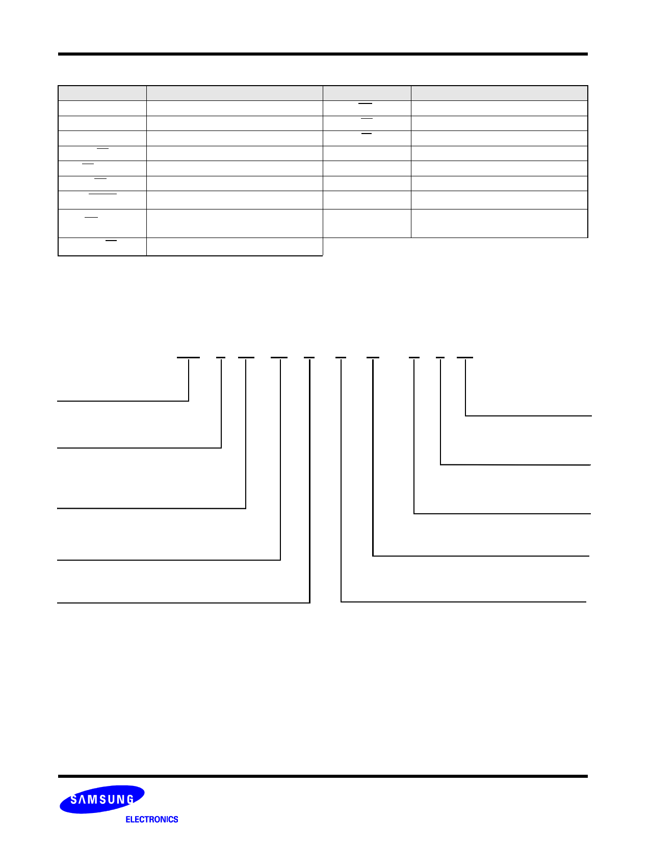
PIN DESCRIPTION
Ball Name
A0ru to A20ru
A21r to A22r
DQ0ru to DQ15ru
CEr
CS1u,CS2u
OEru
RESETr
Description
Address Inputs(Common)
Address Inputs(NOR)
Data Input/output(Common)
Chip Enable (NOR)
Chip Select (UtRAM)
Output Enable (Common)
Hardware Reset (NOR)
WPr/ACCr
Hardware Write Protection/
Program Acceleration(NOR)
RYr/BYr
Ready/Busy Output(NOR)
Preliminary
MCP MEMORY
Ball Name
WEru
UBu
LBu
VCCr
VCCu
VSSru
NC
DNU
Description
Write Enable(Common)
Upper Byte(UtRAM)
Lower Byte(UtRAM)
Power Supply(NOR)
Power Supply(UtRAM)
Ground(Common)
No Connection
Do Not Use
ORDERING INFORMATION
K 5 L 27 31 C A M - D 7 70
Samsung MCP Memory
2Chip MCP
Device Type
L : De-muxed NOR Flash + UtRAM
UtRAM Access Time
70 : 70ns
Flash Access Time
7 : 70ns
NOR Flash Density
27 : 128Mb, x16 ,Page, 1CE
Package
D : FBGA(LF)
UtRAM Density, (Organization)
31 : 32Mb, x16, Page
Version
M : 1st Generation
Operating Voltage
C : 3.0V/3.0V
Block Architecture
A : Top & Bottom Boot Block
www.DataSheet.in
5 Revision 0.0
September 2006
5 Page 
K5L2731CAM-D770
Preliminary
MCP MEMORY
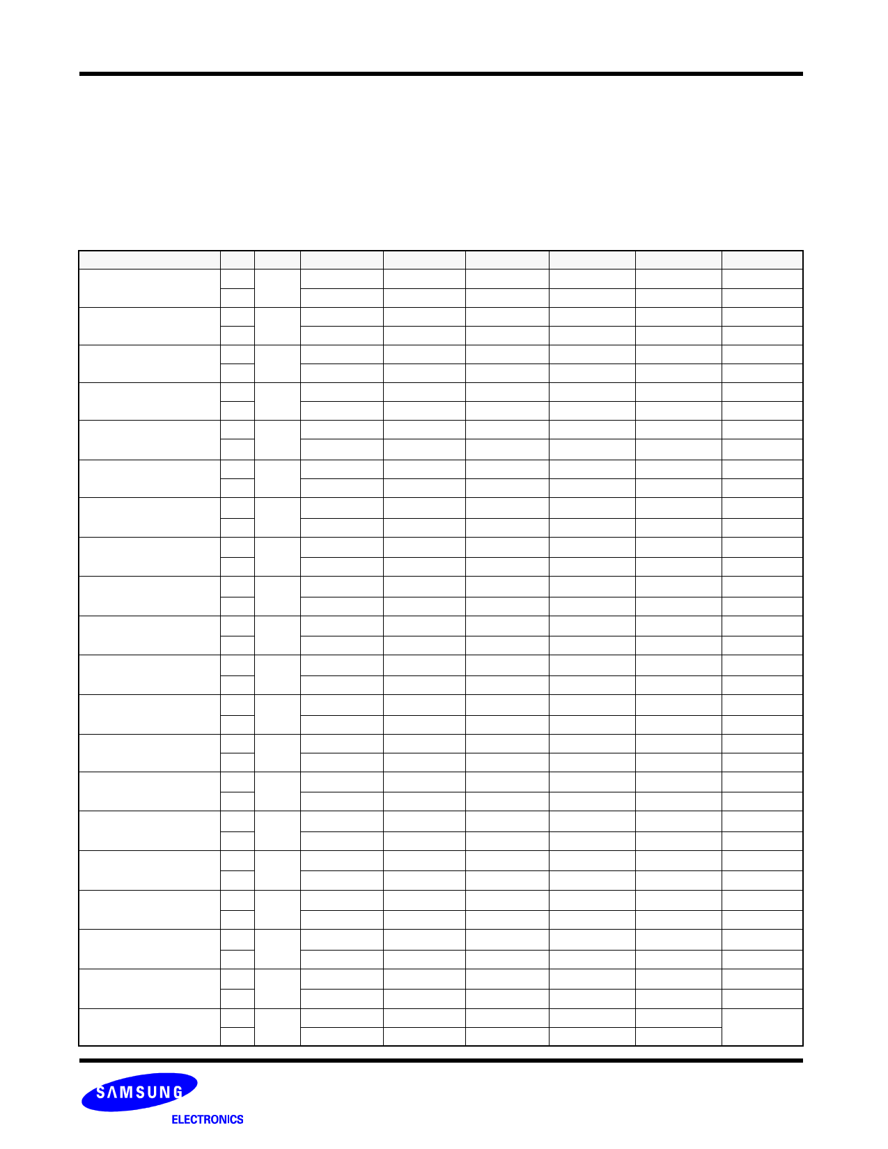
COMMAND DEFINITIONS
The device operates by selecting and executing its operational modes. Each operational mode has its own command set. In order to select a
certain mode, a proper command with specific address and data sequences must be written into the command register. Writing incorrect infor-
mation which include address and data or writing an improper command will reset the device to the read mode. The defined valid register com-
mand sequences are stated in Table 6. Note that Erase Suspend (B0H) and Erase Resume (30H) commands are valid only while the Block
Erase Operation is in progress. Program Suspend (B0H) and Program Resume (30H) commands are valid during Program Operation and
Erase Suspend - Program Operation. Only Read Operation is available after Program Suspend Operation.
Table 6. Command Sequences
Command Sequence
Cycle
Read
Addr
Data
1
Reset
Addr
Data
1
Autoselect
Manufacturer ID (1,2)
Addr
Data
4
Autoselect Device Code
(1,2,3)
Addr
Data
4
Autoselect
Block Protect Verify (1,2)
Addr
Data
4
Autoselect OTP Factory Pro- Addr
tect Data
4
Program
Addr
Data
4
Unlock Bypass
Addr
Data
3
Unlock Bypass
Program
Addr
Data
2
Unlock Bypass
Block Erase
Addr
Data
2
Unlock Bypass Chip Erase
Addr
Data
2
Unlock Bypass Reset
Addr
Data
2
Unlock Bypass CFI
Addr
Data
1
Chip Erase
Addr
Data
6
Block Erase
Addr
Data
6
Block Erase Suspend
(4, 5)
Addr
Data
1
Block Erase Resume
Addr
Data
1
Program Suspend (6,7)
Addr
Data
1
Program Resume
Addr
Data
1
CFI Query (8)
Addr
Data
1
1st Cycle
RA
RD
XXXH
F0H
555H
AAH
555H
AAH
555H
AAH
555H
AAH
555H
AAH
555H
AAH
XXXH
A0H
XXXH
80H
XXXH
80H
XXXH
90H
XXH
98H
555H
AAH
555H
AAH
DA
B0H
DA
30H
DA
B0H
DA
30H
55H
98H
2nd Cycle
2AAH
55H
2AAH
55H
2AAH
55H
2AAH
55H
2AAH
55H
2AAH
55H
PA
PD
BA
30H
XXXH
10H
XXXH
00H
2AAH
55H
2AAH
55H
3rd Cycle
4th Cycle
5th Cycle
DA/555H
90H
DA/555H
90H
DA/555H
90H
DA/555H
90H
555H
A0H
555H
20H
DA/X00H
ECH
DA/X01H
257EH
BA / X02H
(See Table 7)
X03H
(See Note 10)
PA
PD
DA/X0EH
2508H
555H
80H
555H
80H
555H
AAH
555H
AAH
2AAH
55H
2AAH
55H
6th Cycle
DA/X0FH
2501H
555H
10H
BA
30H
11 Revision 0.0
September 2006
www.DataSheet.in
11 Page | ||
| Páginas | Total 30 Páginas | |
| PDF Descargar | [ Datasheet K5L2731CAM-D770.PDF ] | |
Hoja de datos destacado
| Número de pieza | Descripción | Fabricantes |
| K5L2731CAM-D770 | 128Mb NOR Flash + 32Mb UtRAM | Samsung Electronics |
| Número de pieza | Descripción | Fabricantes |
| SLA6805M | High Voltage 3 phase Motor Driver IC. |
Sanken |
| SDC1742 | 12- and 14-Bit Hybrid Synchro / Resolver-to-Digital Converters. |
Analog Devices |
|
DataSheet.es es una pagina web que funciona como un repositorio de manuales o hoja de datos de muchos de los productos más populares, |
| DataSheet.es | 2020 | Privacy Policy | Contacto | Buscar |
