|
|
PDF 45DB642D Data sheet ( Hoja de datos )
| Número de pieza | 45DB642D | |
| Descripción | AT45DB642D | |
| Fabricantes | ATMEL Corporation | |
| Logotipo |  |
|
Hay una vista previa y un enlace de descarga de 45DB642D (archivo pdf) en la parte inferior de esta página. Total 30 Páginas | ||
|
No Preview Available !
Features
• Single 2.7V - 3.6V Supply
• Dual-interface Architecture
– RapidS Serial Interface: 66 MHz Maximum Clock Frequency
SPI Compatible Modes 0 and 3
– Rapid8 8-bit Interface: 50 MHz Maximum Clock Frequency
• User Configurable Page Size
– 1024 Bytes per Page
– 1056 Bytes per Page
– Page Size Can Be Factory Pre-configured for 1024 Bytes
• Page Program Operation
– Intelligent Programming Operation
– 8192 Pages (1024/1056 Bytes/Page) Main Memory
• Flexible Erase Options
– Page Erase (1 Kbyte)
– Block Erase (8 Kbytes)
– Sector Erase (256 Kbytes)
– Chip Erase (64 Mbits)
• Two SRAM Data Buffers (1024/1056 Bytes)
– Allows Receiving of Data while Reprogramming the Flash Array
• Continuous Read Capability through Entire Array
– Ideal for Code Shadowing Applications
• Low-power Dissipation
– 10 mA Active Read Current Typical – Serial Interface
– 10 mA Active Read Current Typical – 8-bit Interface
– 25 µA Standby Current Typical
– 15 µA Deep Power Down Typical
• Hardware and Software Data Protection Features
– Individual Sector
• Permanent Sector Lockdown for Secure Code and Data Storage
– Individual Sector
• Security: 128-byte Security Register
– 64-byte User Programmable Space
– Unique 64-byte Device Identifier
• JEDEC Standard Manufacturer and Device ID Read
• 100,000 Program/Erase Cycles Per Page Minimum
• Data Retention – 20 Years
• Green (Pb/Halide-free/RoHS Compliant) Packaging Options
• Temperature Range
– Industrial: -40°C to +85°C
64-megabit
2.7-volt
Dual-interface
DataFlash®
AT45DB642D
3542K–DFLASH–04/09
1 page 
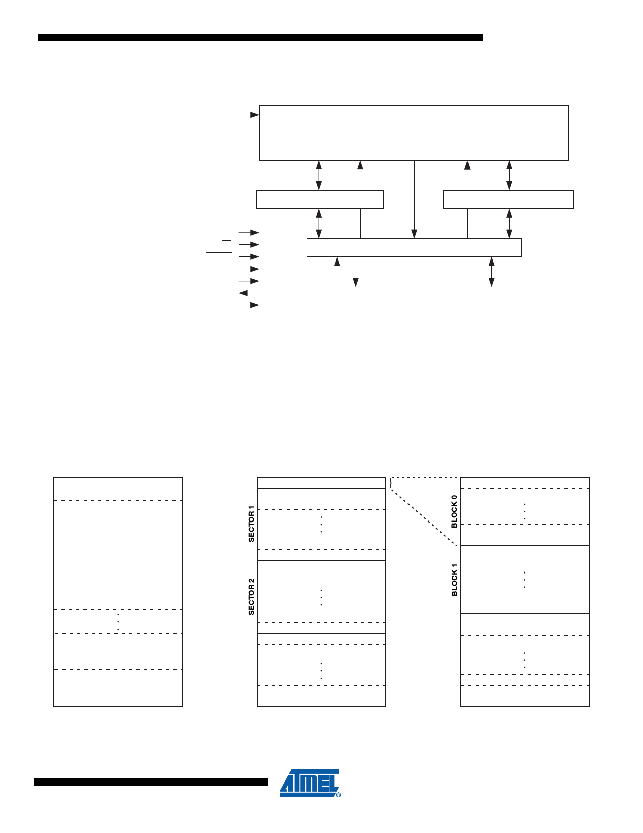
3. Block Diagram
AT45DB642D
WP FLASH MEMORY ARRAY
PAGE (1024/1056 BYTES)
SCK/CLK
CS
RESET
VCC
GND
RDY/BUSY
SER/BYTE
BUFFER 1 (1024/1056 BYTES)
BUFFER 2 (1024/1056 BYTES)
I/O INTERFACE
SI SO
I/O7 - I/O0
4. Memory Array
To provide optimal flexibility, the memory array of the AT45DB642D is divided into three levels of
granularity comprising of sectors, blocks, and pages. The “Memory Architecture Diagram” illus-
trates the breakdown of each level and details the number of pages per sector and block. All
program operations to the DataFlash occur on a page by page basis. The erase operations can
be performed at the chip, sector, block or page level.
Figure 4-1. Memory Architecture Diagram
SECTOR ARCHITECTURE
SECTOR 0a = 8 Pages
8192/8,448 bytes
SECTOR 0b = 248 Pages
253,952/261,888 bytes
SECTOR 0
BLOCK ARCHITECTURE
BLOCK 0
BLOCK 1
BLOCK 2
SECTOR 1 = 256 Pages
262,144/270,336 bytes
SECTOR 2 = 256 Pages
262,144/270,336 bytes
BLOCK 30
BLOCK 31
BLOCK 32
BLOCK 33
SECTOR 30 = 256 Pages
262,144/270,336 bytes
BLOCK 62
BLOCK 63
BLOCK 64
BLOCK 65
8 Pages
PAGE ARCHITECTURE
PAGE 0
PAGE 1
PAGE 6
PAGE 7
PAGE 8
PAGE 9
PAGE 14
PAGE 15
PAGE 16
PAGE 17
PAGE 18
SECTOR 31 = 256 Pages
262,144/270,336 bytes
BLOCK 1022
BLOCK 1023
Block = 8,192/8,448 bytes
PAGE 8,190
PAGE 8,190
Page = 1,024/1,056 bytes
3542K–DFLASH–04/09
5
5 Page 
AT45DB642D
7.6 Sector Erase
The Sector Erase command can be used to individually erase any sector in the main memory.
There are 32 sectors and only one sector can be erased at one time. To perform sector 0a or
sector 0b erase for the standard DataFlash page size (1056 bytes), an opcode of 7CH must be
loaded into the device, followed by three address bytes comprised of 10 page address bits
(PA12 - PA3) and 14 don’t care bits. To perform a sector 1-31 erase, the opcode 7CH must be
loaded into the device, followed by three address bytes comprised of 5 page address bits (PA12
- PA8) and 19 don’t care bits. To perform sector 0a or sector 0b erase for the binary page size
(1024 bytes), an opcode of 7CH must be loaded into the device, followed by three address bytes
comprised of 1 don’t care bit and 10 page address bits (A22 - A13) and 13 don’t care bits. To
perform a sector 1-31 erase, the opcode 7CH must be loaded into the device, followed by three
address bytes comprised of 1 don’t care bit and 5 page address bits (PA12 - PA8) and 18 don’t
care bits. The page address bits are used to specify any valid address location within the sector
which is to be erased. When a low-to-high transition occurs on the CS pin, the part will erase the
selected sector. The erase operation is internally self-timed and should take place in a maximum
time of tSE. During this time, the status register and the RDY/BUSY pin will indicate that the part
is busy.
Table 7-2. Sector Erase Addressing
PA12/ PA11/ PA10/ PA9/
A22 A21 A20 A19
PA8/
A18
00000
00000
00001
00010
•••••
•••••
•••••
11100
11101
11110
11111
PA7/
A17
0
0
X
X
•
•
•
X
X
X
X
PA6/
A16
0
0
X
X
•
•
•
X
X
X
X
PA5/
A15
0
0
X
X
•
•
•
X
X
X
X
PA4/
A14
0
0
X
X
•
•
•
X
X
X
X
PA3/
A13
0
1
X
X
•
•
•
X
X
X
X
PA2/
A12
X
X
X
X
•
•
•
X
X
X
X
PA1/
A11
X
X
X
X
•
•
•
X
X
X
X
PA0/
A10
X
X
X
X
•
•
•
X
X
X
X
Sector
0a
0b
1
2
•
•
•
28
29
30
31
7.7 Chip Erase(1)
The entire main memory can be erased at one time by using the Chip Erase command.
To execute the Chip Erase command, a 4-byte command sequence C7H, 94H, 80H and 9AH
must be clocked into the device. Since the entire memory array is to be erased, no address
bytes need to be clocked into the device, and any data clocked in after the opcode will be
ignored. After the last bit of the opcode sequence has been clocked in, the CS pin can be deas-
serted to start the erase process. The erase operation is internally self-timed and should take
place in a time of tCE. During this time, the Status Register will indicate that the device is busy.
The Chip Erase command will not affect sectors that are protected or locked down; the contents
of those sectors will remain unchanged. Only those sectors that are not protected or locked
down will be erased.
3542K–DFLASH–04/09
11
11 Page | ||
| Páginas | Total 30 Páginas | |
| PDF Descargar | [ Datasheet 45DB642D.PDF ] | |
Hoja de datos destacado
| Número de pieza | Descripción | Fabricantes |
| 45DB642D | AT45DB642D | ATMEL Corporation |
| Número de pieza | Descripción | Fabricantes |
| SLA6805M | High Voltage 3 phase Motor Driver IC. |
Sanken |
| SDC1742 | 12- and 14-Bit Hybrid Synchro / Resolver-to-Digital Converters. |
Analog Devices |
|
DataSheet.es es una pagina web que funciona como un repositorio de manuales o hoja de datos de muchos de los productos más populares, |
| DataSheet.es | 2020 | Privacy Policy | Contacto | Buscar |
