|
|
|
PDF FS6131 Data sheet ( Hoja de datos )
| Número de pieza | FS6131 | |
| Descripción | Programmable Line Lock Clock Generator IC | |
| Fabricantes | ON Semiconductor | |
| Logotipo | ||
Hay una vista previa y un enlace de descarga de FS6131 (archivo pdf) en la parte inferior de esta página. Total 44 Páginas | ||
|
No Preview Available !
FS6131
Programmable Line Lock Clock Generator IC
1.0 Key Features
• Complete programmable control via I2C™-bus
• Selectable CMOS or PECL compatible outputs
• External feedback loop capability allows genlocking
• Tunable VCXO loop for jitter attenuation
2.0 General Description
The FS6131-01 is a monolithic CMOS clock generator/regenerator IC designed to minimize cost and component count in a variety of
electronic systems. Via the I2C-bus interface, the FS6131-01 can be adapted to many clock generation requirements.
The ability to tune the on-board voltage-controlled crystal oscillator (VCXO), the length of the reference and feed-back dividers, their
granularity, and the flexibility of the post divider make the FS6131-01 the most flexible stand-alone phase-locked loop (PLL) clock
generator available.
3.0 Applications
• Frequency synthesis
• Line-locked and genlock applications
• Clock multiplication
• Telecom jitter attenuation
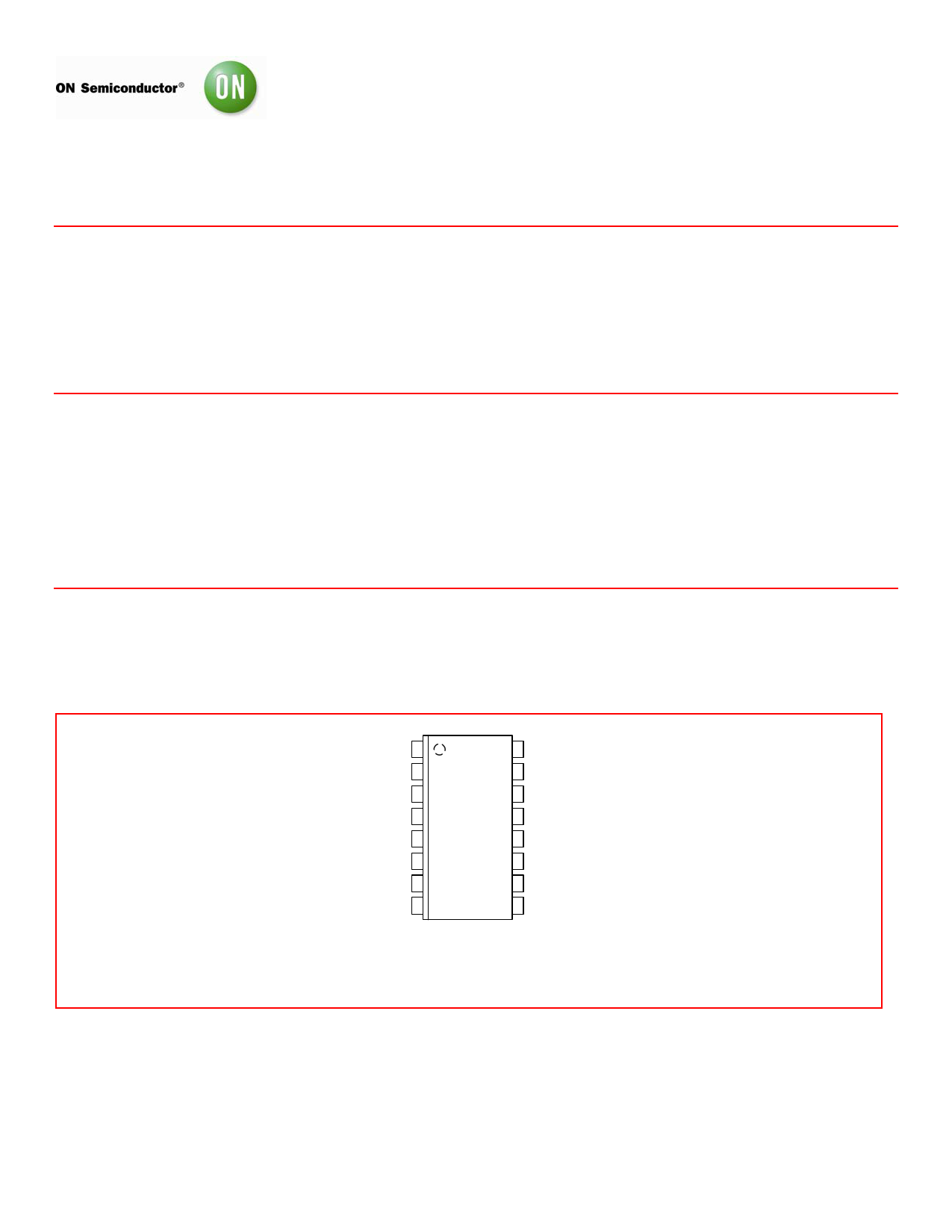
SCL 1
SDA 2
ADDR 3
VSS 4
XIN 5
XOUT 6
XTUNE 7
VDD 8
16 CLKN
15 CLKP
14 VDD
13 FBK
12 REF
11 VSS
10 EXTLF
9 LOCK/IPRG
16-pin 0.150" SOIC
Figure 1: Pin Configuration
©2008 SCILLC. All rights reserved.
May 2008 – Rev. 4
www.DataSheet.in
Publication Order Number:
FS6131/D
1 page 
FS6131
4.1.4. Post Divider
The post divider consists of three individually programmable dividers, as shown in Error! Reference source not found..
fGBL
POST1[1:0]
POST2[1:0]
POST3[1:0]
Post
Divider 1
(NP1)
Post
Divider 2
(NP2)
Post
Divider 3
(NP3)
POST DIVIDER (NPx)
Figure 4: Post Divider
fout
The moduli of the individual dividers are denoted as NP1, NP2, and NP3, and together they make up the array modulus NPx.
N Px = N P1 × N P2 × N P3
The post divider performs several useful functions. First, it allows the VCO to be operated in a narrower range of speeds compared to
the variety of output clock speeds that the device is required to generate. Second, it changes the basic PLL equation to
fCLK
=
f REF
⎜⎜⎝⎛
NF
NR
⎟⎟⎠⎞⎜⎜⎝⎛
1
N Px
⎟⎟⎠⎞
The extra integer in the denominator permits more flexibility in the programming of the loop for many applications where frequencies
must be achieved exactly.
Note that a nominal 50/50 duty factor is preserved for selections which have an odd modulus.
4.2 Phase Adjust and Sampling
In line-locked or genlocked applications, it is necessary to know the exact phase relation of the output clock relative to the input clock.
Since the VCO is included within the feedback loop in a simple PLL structure, the VCO output is exactly phase aligned with the input
clock. Every cycle of the input clock equals NR/NF cycles of the VCO clock.
fIN
Reference
Divider (NR)
fIN
fOUT
Phase
Frequency
Detect
VCO
Feedback
Divider (NF)
Figure 5: Simple PLL
fOUT
The addition of a post divider, while adding flexibility, makes the phase relation between the input and output clock unknown because
the post divider is outside the feedback loop.
Rev. 4 | Page 5 of 44 | www.onsemi.com
www.DataSheet.in
5 Page 
FS6131
4.5 Crystal Loop
The crystal loop is designed to attenuate the jitter on a highly jittered, low-Q, low frequency reference. The crystal loop can also
maintain a constant frequency output into the main loop if the low frequency reference is intermittent.
The crystal loop consists of a voltage-controllable crystal oscillator (VCXO), a divider, a PFD, and a charge pump that tunes the VCXO
to a frequency reference. The frequency reference is phase-locked to the divided frequency of an external, high-Q, jitter-free crystal,
thereby locking the VCXO to the reference frequency. The VCXO can continue to run off the crystal even if the frequency reference
becomes intermittent.
4.5.1. Locking to an External Frequency Source
When the crystal loop is synchronized to an external frequency source, the FS6131 can monitor the crystal loop and detect if the loop
unlocks from the external source. The crystal loop tries to drive to zero frequency if the external source is dropped, and sets a lock
status error flag.
The crystal loop can also detect if the VCXO has dropped out of the fine tune range, requiring a change to the coarse tune. The lock
status also latches the direction the loop went out of range (high or low) when the loop became unlocked.
4.5.1.1 Crystal Loop Lock Status Flag
To enable this mode, clear the STAT[1] and STAT[0] bits to zero. If the CMOS bit is set to one, the LOCK/IPRG pin will be low if the
crystal loop becomes unlocked. The flag is always available under software control by reading back the STAT[1] bit, which is
overwritten with the status flag (low = unlocked) in this mode (see Table 6).
4.5.1.2 Out-Of-Range High/Low
The direction the loop has gone out-of-range can be determined by clearing STAT[1] to zero and setting STAT[0] bit to one. If the
CMOS bit is set to one, the LOCK/IPRG pin will go high if the crystal loop went out of range high. If the pin goes to a logic-low, the loop
went out of range low.
The out-of-range information is also available under software control by reading back the STAT[1] bit, which is overwritten by the flag
(high = outof-range high, low = out-of-range low) in this mode. The bit is set or cleared only if the crystal loop loses lock (see Table 6).
4.5.1.3 Crystal Loop Disable
The crystal loop is disabled by setting the XLPDEN bit to a logic-high (1). The bit disables the charge pump circuit in the loop.
Setting the XLPDEN bit low (0) permits the crystal loop to operate as a control loop.
4.6 Connecting the FS6131 to an External Reference Frequency
If a crystal oscillator is not used, tie XIN to ground and shut down the crystal oscillator by setting XLROM[2:0]=1.
The REF and FBK pins do not have pull-up or pull-down current, but do have a small amount of hysteresis to reduce the possibility of
extra edges. Signals may be AC-coupled into these inputs with an external DC-bias circuit to generate a DC-bias of 2.5V. Any
reference or feedback signal should be square for best results, and the signals should be rail-to-rail. Unused inputs should be grounded
to avoid unwanted signal injection.
4.7 Differential Output Stage
The differential output stage supports both CMOS and pseudo-ECL (PECL) signals. The desired output interface is chosen via the
program registers (see Table 4).
If a PECL interface is used, the transmission line is usually terminated using a Thévenin termination. The output stage can only sink
current in the PECL mode, and the amount of sink current is set by a programming resistor on the LOCK/IPRG pin. The ratio of IPRG
current to output drive current is shown in Figure 12. Source current is provided by the pull-up resistor that is part of the Thévenin
termination.
www.DataSheet.in
Rev. 4 | Page 11 of 44 | www.onsemi.com
11 Page | ||
| Páginas | Total 44 Páginas | |
| PDF Descargar | [ Datasheet FS6131.PDF ] | |
Hoja de datos destacado
| Número de pieza | Descripción | Fabricantes |
| FS6131 | Programmable Line Lock Clock Generator IC | ON Semiconductor |
| FS6131-01 | Programmable Line Lock Clock Generator IC | AMI |
| Número de pieza | Descripción | Fabricantes |
| SLA6805M | High Voltage 3 phase Motor Driver IC. |
Sanken |
| SDC1742 | 12- and 14-Bit Hybrid Synchro / Resolver-to-Digital Converters. |
Analog Devices |
|
DataSheet.es es una pagina web que funciona como un repositorio de manuales o hoja de datos de muchos de los productos más populares, |
| DataSheet.es | 2020 | Privacy Policy | Contacto | Buscar |