|
|
|
PDF QLX4270-DP Data sheet ( Hoja de datos )
| Número de pieza | QLX4270-DP | |
| Descripción | DisplayPort Lane Extender | |
| Fabricantes | Intersil Corporation | |
| Logotipo | ||
Hay una vista previa y un enlace de descarga de QLX4270-DP (archivo pdf) en la parte inferior de esta página. Total 7 Páginas | ||
|
No Preview Available !
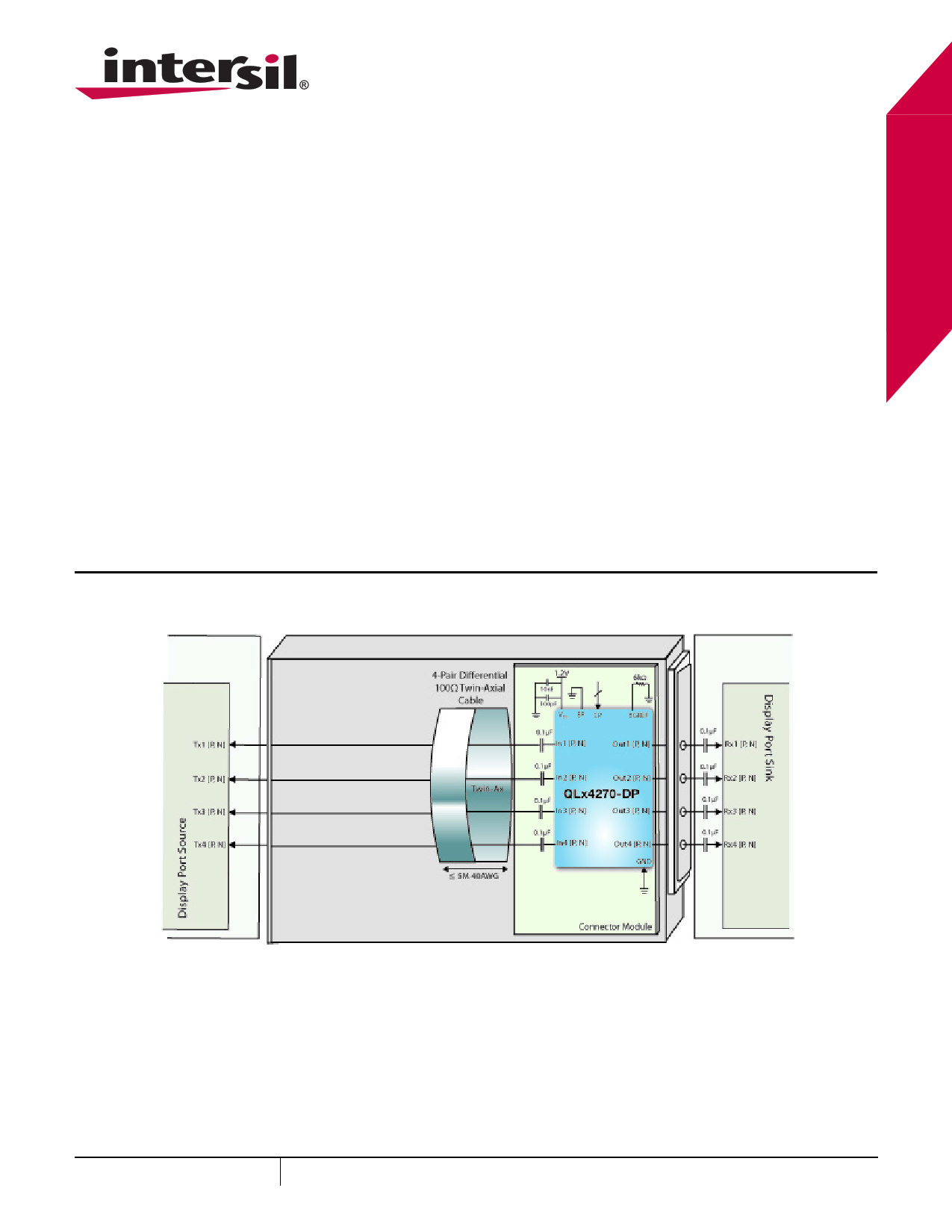
DisplayPort Lane Extender
QLx4270-DP
The QLx4270-DP is a settable quad receive-side
equalizer with extended functionality for DisplayPort
applications. The QLx4270-DP compensates for the
frequency dependent attenuation of copper cables,
allowing operation on ultra-thin 40AWG cable.
The small form factor, highly-integrated quad design is
ideal for high-density data transmission applications
including active copper cable assemblies.
Operating on a single 1.2V power supply, the
QLx4270-DP enables per channel throughputs of up to
2.7Gb/s. The QLx4270-DP uses current mode logic (CML)
inputs/outputs and is packaged in a 4mmx7mm 46 lead
QFN.
Features
• Supports data rates up to 2.7Gb/s per lane
• Low power (78mW per channel)
• Low latency (<500ps)
• Four equalizers in a 4mmx7mm QFN package for
straight route-through architecture and simplified
routing
• Each equalizer boost is independently pin selectable
and programmable
• 1.2V supply voltage
Applications
• DisplayPort (VESA DisplayPort Standard v1.1a)
• DisplayPort adaptors and repeaters
Benefits
• Thinner gauge cable
• Extends cable reach greater than 5x
• Improved BER
Typical Application Circuit
November 19, 2009
FN6972.1
www.DataSheet.in
1 CAUTION: These devices are sensitive to electrostatic discharge; follow proper IC Handling Procedures.
1-888-INTERSIL or 1-888-468-3774 | Intersil (and design) is a registered trademark of Intersil Americas Inc.
Copyright Intersil Americas Inc. 2009. All Rights Reserved
All other trademarks mentioned are the property of their respective owners.
1 page 
QLx4270-DP
Electrical Characteristics VDD = 1.2V, TA = +25°C, and VIN = 800mVP-P, unless otherwise noted. (Continued)
PARAMETER
SYMBOL
CONDITION
MIN TYP MAX UNITS NOTES
Output Return Loss
(Com. to Diff.
Conversion)
SDC22 50MHz to 1.35GHz
20 dB 4
Output Residual Jitter
2.7Gb/s; Up to 2m 38AWG standard twin-axial
cable (11.5dB loss)
0.15 0.2
UI 3, 5, 6
Output Transition Time
Lane-to-Lane Skew
tr, tf
20% to 80%
30 60 100
50
ps
ps
7
Propagation Delay
From IN[k] to OUT[k]
500 ps
NOTES:
3. After channel loss, differential amplitudes at QLx4270-DP inputs must meet the input voltage range specified in “Absolute
Maximum Ratings” on page 4.
4. Temperature = +25°C, VDD = 1.2V.
5. Output residual jitter is the difference between the total jitter at the lane extender output and the total jitter of the transmitted
signal (as measured at the input to the channel). Total jitter (TJ) is DJpp + 14.1 x RJRMS.
6. Measured using a PRBS 27-1 pattern. Deterministic jitter at the input to the lane extender is due to frequency-dependent,
media-induced loss only.
7. Rise and fall times measured using a 1GHz clock with a 20ps edge rate.
Control Pin Boost Setting
The voltages at the CP pins are used to determine the
boost level of each channel of QLx4270-DP. For each of
the four channels, k, the [A], [B], and [C] control pins
(CP[k]) are associated with a 3-bit non binary word.
While [A] can take one of two values, ‘LOW’ or ‘HIGH’,
[B] and [C] can take one of three different values: ‘LOW’,
‘MIDDLE’, or ‘HIGH’. This is achieved by changing the
value of a resistor connected between VDD and the CP
pin, which is internally pulled low with a 25kΩ resistor.
Thus, a ‘HIGH’ state is achieved by using a 0Ω resistor,
‘MIDDLE’ is achieved with a 25kΩ resistor, and ‘LOW’ is
achieved with an open resistance. Table 1 defines the
mapping from the 3-bit CP word to the 18 out of 32
possible levels available via the serial interface on the
Evaluation Board kit.
TABLE 1. MAPPING BETWEEN CP-SETTING RESISTOR
AND QLx4270-DP BOOST LEVELS
RESISTANCE BETWEEN CP PIN
AND VDD
CP[A]
CP[B]
CP[C]
SERIAL BOOST
LEVEL
Open
Open
Open
0
Open
Open
Open
Open
25kΩ
0Ω
2
4
Open
Open
25kΩ
25kΩ
Open
25kΩ
6
8
Open
Open
25kΩ
0Ω
0Ω
Open
10
12
Open
Open
0Ω 25kΩ
0Ω 0Ω
14
15
0Ω
Open
Open
16
TABLE 1. MAPPING BETWEEN CP-SETTING RESISTOR
AND QLx4270-DP BOOST LEVELS (Continued)
RESISTANCE BETWEEN CP PIN
AND VDD
CP[A]
CP[B]
CP[C]
SERIAL BOOST
LEVEL
0Ω
Open
25kΩ
17
0Ω
Open
0Ω
19
0Ω
25kΩ
Open
21
0Ω
25kΩ
25kΩ
23
0Ω
25kΩ
0Ω
24
0Ω 0Ω Open 26
0Ω 0Ω 25kΩ 28
0Ω 0Ω 0Ω
31
If all four channels are to use the same boost level, then
a minimum number of board resistors can be realized by
tying together like CP[k][A,B,C] pins across all channels
k. For instance, all four CP[k][A] pins can be tied to the
same resistor running to VDD. Consequently, only three
resistors are needed to control the boost of all four
channels. If the CP Pins are tied together and the 25kΩ is
used, the value changes to a 3.125kΩ resistor because
the 25kΩ is divided by 4.
Channel Power-Down
The IS[k] pin powers down the equalizer channel when
pulled low. This feature allows individually to power down
unused channels and to minimize power consumption.
Example: for DisplayPort applications with 1 or 2 links,
the unused channels may be powered down to save
power. The current draw for a channel is reduced from
50mA to 3.8mA when powered down.
5 FN6972.1
November 19, 2009
www.DataSheet.in
5 Page | ||
| Páginas | Total 7 Páginas | |
| PDF Descargar | [ Datasheet QLX4270-DP.PDF ] | |
Hoja de datos destacado
| Número de pieza | Descripción | Fabricantes |
| QLX4270-DP | DisplayPort Lane Extender | Intersil Corporation |
| Número de pieza | Descripción | Fabricantes |
| SLA6805M | High Voltage 3 phase Motor Driver IC. |
Sanken |
| SDC1742 | 12- and 14-Bit Hybrid Synchro / Resolver-to-Digital Converters. |
Analog Devices |
|
DataSheet.es es una pagina web que funciona como un repositorio de manuales o hoja de datos de muchos de los productos más populares, |
| DataSheet.es | 2020 | Privacy Policy | Contacto | Buscar |