|
|
|
PDF AD5421 Data sheet ( Hoja de datos )
| Número de pieza | AD5421 | |
| Descripción | 4mA to 20mA DAC | |
| Fabricantes | Analog Devices | |
| Logotipo | ||
1. AD5421 Hay una vista previa y un enlace de descarga de AD5421 (archivo pdf) en la parte inferior de esta página. Total 30 Páginas | ||
|
No Preview Available !
Data Sheet
16-Bit, Serial Input,
Loop-Powered, 4 mA to 20 mA DAC
AD5421
FEATURES
GENERAL DESCRIPTION
16-bit resolution and monotonicity
Pin selectable NAMUR-compliant ranges
4 mA to 20 mA
3.8 mA to 21 mA
3.2 mA to 24 mA
NAMUR-compliant alarm currents
Downscale alarm current = 3.2 mA
Upscale alarm current = 22.8 mA/24 mA
Total unadjusted error (TUE): 0.05% maximum
INL error: 0.0035% FSR maximum
Output TC: 3 ppm/°C typical
Quiescent current: 300 µA maximum
Flexible SPI-compatible serial digital interface
with Schmitt triggered inputs
On-chip fault alerts via FAULT pin or alarm current
Automatic readback of fault register on each write cycle
Slew rate control function
Gain and offset adjust registers
On-chip reference TC: 4 ppm/°C maximum
Selectable regulated voltage output
Loop voltage range: 5.5 V to 52 V
Temperature range: −40°C to +105°C
TSSOP and LFCSP packages
APPLICATIONS
Industrial process control
4 mA to 20 mA loop-powered transmitters
Smart transmitters
HART network connectivity
The AD5421 is a complete, loop-powered, 4 mA to 20 mA
digital-to-analog converter (DAC) designed to meet the needs
of smart transmitter manufacturers in the industrial control
industry. The DAC provides a high precision, fully integrated,
low cost solution in compact TSSOP and LFCSP packages.
The AD5421 includes a regulated voltage output that is used to
power itself and other devices in the transmitter. This regulator
provides a regulated 1.8 V to 12 V output voltage. The AD5421
also contains 1.22 V and 2.5 V references, thus eliminating the
need for a discrete regulator and voltage reference.
The AD5421 can be used with standard HART® FSK protocol
communication circuitry without any degradation in specified
performance. The high speed serial interface is capable of operating
at 30 MHz and allows for simple connection to commonly used
microprocessors and microcontrollers via a SPI-compatible, 3-wire
interface.
The AD5421 is guaranteed monotonic to 16 bits. It provides
0.0015% integral nonlinearity, 0.0012% offset error, and
0.0006% gain error under typical conditions.
The AD5421 is available in a 28-lead TSSOP and a 32-lead LFCSP
specified over the extended industrial temperature range of
−40°C to +105°C.
COMPANION LOW POWER PRODUCTS
HART Modem: AD5700, AD5700-1
Microcontroller: ADuCM360
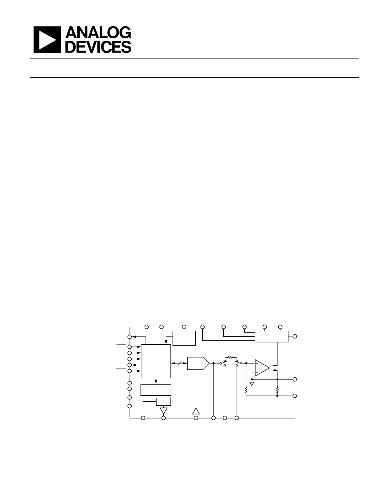
FUNCTIONAL BLOCK DIAGRAM
IODVDD DVDD
VLOOP REG_SEL0 REG_SEL1 REG_SEL2 REGOUT REGIN
FAULT
SYNC
SCLK
SDIN
SDO
LDAC
RANGE0
RANGE1
ALARM_CURRENT_DIRECTION
RINT/REXT
INPUT
REGISTER
CONTROL
LOGIC
GAIN/OFFSET
ADJUSTMENT
REGISTERS
LOOP
VOLTAGE
MONITOR
16 16-BIT
DAC
TEMPERATURE
SENSOR
VREF
RSET
24kΩ
VOLTAGE
REGULATOR
DRIVE
11.5kΩ 52Ω
AD5421
COM
LOOP–
REFOUT2 REFOUT1
REFIN
Figure 1.
CIN REXT1 REXT2
Rev. H
Document Feedback
Information furnished by Analog Devices is believed to be accurate and reliable. However, no
responsibility is assumed by Analog Devices for its use, nor for any infringements of patents or other
rights of third parties that may result from its use. Specifications subject to change without notice. No
license is granted by implication or otherwise under any patent or patent rights of Analog Devices.
Trademarksandregisteredtrademarksarethepropertyoftheirrespectiveowners.
One Technology Way, P.O. Box 9106, Norwood, MA 02062-9106, U.S.A.
Tel: 781.329.4700 ©2011–2014 Analog Devices, Inc. All rights reserved.
Technical Support
www.analog.com
1 page 
AD5421
Data Sheet
SPECIFICATIONS
Loop voltage = 24 V; REFIN = 2.5 V external; RL = 250 Ω; external NMOS connected; all loop current ranges; all specifications
TMIN to TMAX, unless otherwise noted.
Table 1.
Parameter1
ACCURACY, INTERNAL RSET
Resolution
Total Unadjusted Error (TUE)2
TUE Long-Term Stability
Relative Accuracy (INL)
Differential Nonlinearity (DNL)
Offset Error
Offset Error TC3
Gain Error
Gain Error TC3
Full-Scale Error
Full-Scale Error TC3
Downscale Alarm Current
Upscale Alarm Current
ACCURACY, EXTERNAL RSET (24 kΩ)
Resolution
Total Unadjusted Error (TUE)2
TUE Long-Term Stability
Relative Accuracy (INL)
Differential Nonlinearity (DNL)
Offset Error
Offset Error TC3
Gain Error
Min
16
−0.126
−0.041
−0.18
−0.06
−0.27
−0.08
−0.0035
−0.012
−0.024
−1
−0.056
−0.008
−0.11
−0.107
−0.035
−0.2
−0.126
−0.041
−0.25
3.19
22.77
23.97
16
−0.048
−0.027
−0.08
−0.04
−0.0035
−0.012
−1
−0.021
−0.007
−0.03
−0.023
Typ
±0.0064
±0.011
±0.011
210
±0.0015
±0.006
±0.01
±0.0008
±0.0008
1
±0.0058
±0.0058
4
±0.0065
±0.0065
5
±0.002
±0.003
40
±0.0015
±0.006
±0.0012
0.5
±0.0006
Max
+0.126
+0.041
+0.18
+0.06
+0.27
+0.08
+0.0035
+0.012
+0.024
+1
+0.056
+0.008
+0.11
+0.107
+0.035
+0.2
+0.126
+0.041
+0.25
3.21
22.83
24.03
+0.048
+0.027
+0.08
+0.04
+0.0035
+0.012
+1
+0.021
+0.007
+0.03
+0.023
Unit Test Conditions/Comments
Bits
% FSR
% FSR
% FSR
% FSR
% FSR
ppm FSR
% FSR
% FSR
% FSR
LSB
% FSR
% FSR
% FSR
ppm FSR/°C
% FSR
% FSR
% FSR
ppm FSR/°C
% FSR
% FSR
% FSR
ppm FSR/°C
mA
mA
mA
Bits
% FSR
% FSR
% FSR
% FSR
ppm FSR
% FSR
% FSR
LSB
% FSR
% FSR
ppm FSR/°C
% FSR
% FSR
C grade
C grade, TA = 25°C
B grade
B grade, TA = 25°C
A grade
A grade, TA = 25°C
Drift after 1000 hours at TA = 125°C
C grade
B grade
A grade
Guaranteed monotonic
B grade and C grade
B grade and C grade, TA = 25°C
A grade
B grade and C grade
B grade and C grade, TA = 25°C
A grade
B grade and C grade
B grade and C grade, TA = 25°C
A grade
4 mA to 20 mA and 3.8 mA to 21 mA
ranges
3.2 mA to 24 mA range
Assumes ideal resistor, B grade and
C grade only; not specified for A grade
C grade
C grade, TA = 25°C
B grade
B grade, TA = 25°C
Drift after 1000 hours at TA = 125°C
C grade
B grade
Guaranteed monotonic
TA = 25°C
TA = 25°C
Rev. H | Page 4 of 36
5 Page 
AD5421
Timing Diagrams
SCLK
SDIN
SDO
SYNC
LDAC
t12 t1
1 2 8 9 10 11 12 22 23 24
t3 t2
D23 D16 D15 D14 D13
t4
t6
t7
t8
D15 D14 D13
t11
D2 D1 D0
D2 D1
D0
t5
t13
t9 t10
Figure 2. Serial Interface Timing Diagram
Data Sheet
SCLK
SDIN
SDO
SYNC
1
89
24
D23 D16 D15
D0
INPUT WORD SPECIFIES REGISTER TO BE READ
UNDEFINED DATA
1 8 9 24
D23 D16 D15
D0
NOP OR REGISTER ADDRESS
D15 D0
SPECIFIED REGISTER DATA CLOCKED OUT
Figure 3. Readback Timing Diagram
200µA
IOL
TO OUTPUT
PIN CL
30pF
VOH (MIN) OR
VOL (MAX)
200µA
IOH
Figure 4. SDO Load Diagram
Rev. H | Page 10 of 36
11 Page | ||
| Páginas | Total 30 Páginas | |
| PDF Descargar | [ Datasheet AD5421.PDF ] | |
Hoja de datos destacado
| Número de pieza | Descripción | Fabricantes |
| AD542 | High Performance/ BiFET Operational Amplifiers | Analog Devices |
| AD5420 | Current Source DAC | Analog Devices |
| AD5421 | 4mA to 20mA DAC | Analog Devices |
| AD5422 | (AD5412 / AD5422) Current Source & Voltage Output DAC | Analog Devices |
| Número de pieza | Descripción | Fabricantes |
| SLA6805M | High Voltage 3 phase Motor Driver IC. |
Sanken |
| SDC1742 | 12- and 14-Bit Hybrid Synchro / Resolver-to-Digital Converters. |
Analog Devices |
|
DataSheet.es es una pagina web que funciona como un repositorio de manuales o hoja de datos de muchos de los productos más populares, |
| DataSheet.es | 2020 | Privacy Policy | Contacto | Buscar |