|
|
|
PDF NCP3125 Data sheet ( Hoja de datos )
| Número de pieza | NCP3125 | |
| Descripción | 4 A Synchronous PWM Switching Converter | |
| Fabricantes | ON Semiconductor | |
| Logotipo | ||
Hay una vista previa y un enlace de descarga de NCP3125 (archivo pdf) en la parte inferior de esta página. Total 22 Páginas | ||
|
No Preview Available !
NCP3125
www.DataSheet4U.com
4 A Synchronous PWM
Switching Converter
The NCP3125 is a flexible synchronous PWM Switching Buck
Regulator. The NCP3125 is capable of producing output voltages as
low as 0.8 V. The NCP3125 also incorporates voltage mode control.
To reduce the number of external components, a number of features
are internally set including switching frequency. The NCP3125 is
currently available in an SOIC−8 package.
Features
• 4.5 V to 13.2 V Operating Input Voltage Range
• 60 mW High−Side, 36 mW Low−Side Switches
• Output Voltage Adjustable to 0.8 V
• 4 A Continuous Output Current
• Fixed 350 kHz PWM Operation
• 1.0% Initial Output Accuracy
• 75% Max Duty Ratio
• Short−Circuit Protection
• Programmable Current Limit
• This is a Pb−Free Device
Typical Application
• Set Top Boxes
• DVD Drives and HDD
• LCD Monitors and TVs
• Cable Modems
• Telecom / Networking / Datacom Equipment
http://onsemi.com
8
1
SOIC−8 NB
D SUFFIX
CASE 751
MARKING
DIAGRAM
8
3125
ALYWXG
G
1
3125
A
L
Y
W
G
= Specific Device Code
= Assembly Location
= Wafer Lot
= Year/
= Work Week
= Pb−Free Package
PIN CONNECTIONS
PGND
FB
COMP
AGND
1
(Top View)
VSW
ISET
VIN
BST
ORDERING INFORMATION
See detailed ordering and shipping information in the package
dimensions section on page 21 of this data sheet.
4.5 V − 13.2 V
VIN
BST
VSW
PGND
NCP3125
ISET
FB1
COMP
AGND
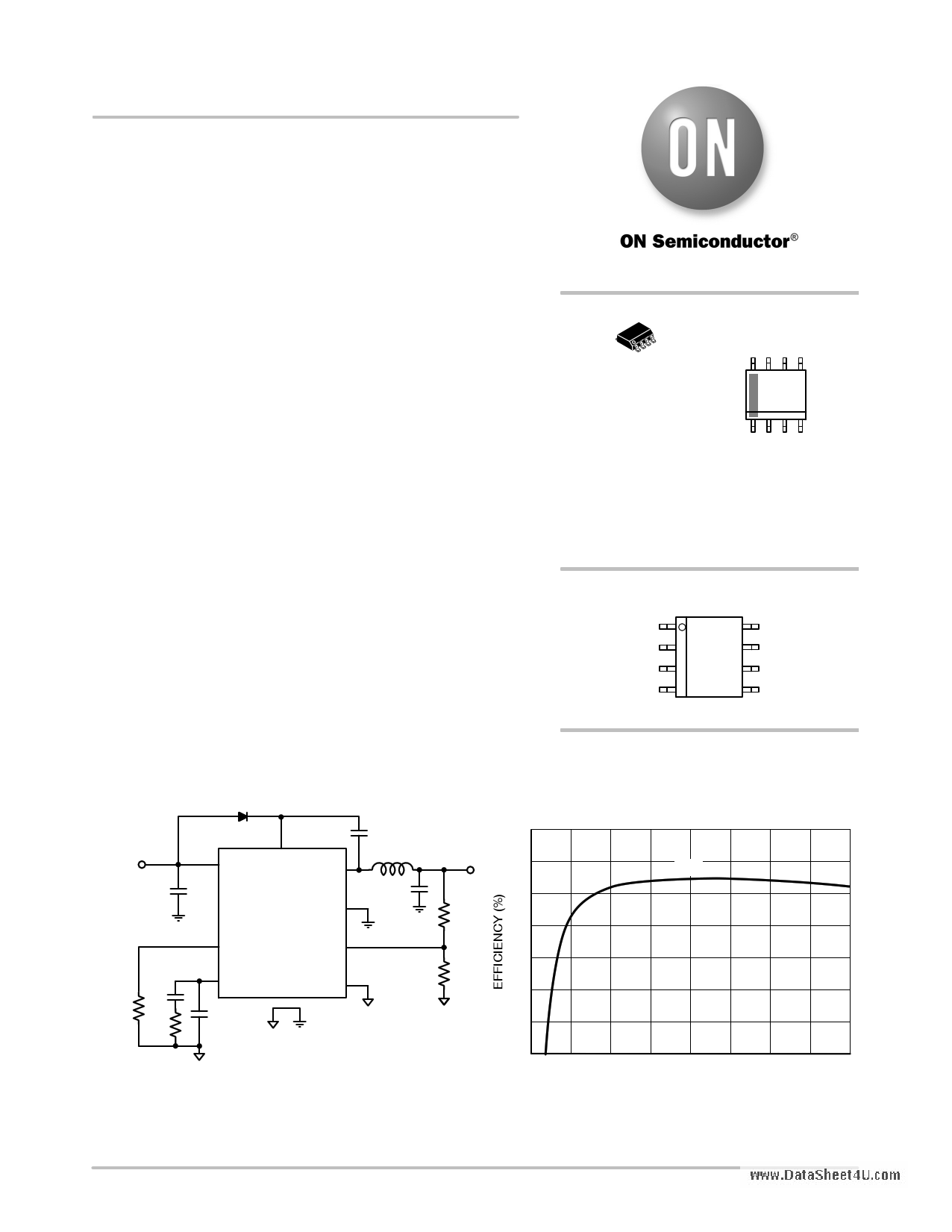
Figure 1. Typical Application Circuit
3.3 V
100
95 5 V
90
85
80
75
70
65
0 0.5 1 1.5 2 2.5 3 3.5 4
OUTPUT CURRENT (A)
Figure 2. Efficiency (VIN = 12 V) vs. Load Current
© Semiconductor Components Industries, LLC, 2010
April, 2010 − Rev. 1
1
Publication Order Number:
NCP3125/D
1 page 
NCP3125
TYPICAL CHARACTERISTICS
www.DataSheet4U.com
5.0
4.5
4.0
VCC = 12 V
3.5
3.0
VCC = 5 V
2.5
2.0
−60 −40 −20 0 20 40 60 80 100 120 140
TJ, JUNCTION TEMPERATURE (°C)
Figure 4. ICC vs. Temperature
14
13
12
11
25
23
21
19
17
15
13
11
9
0
808
806
804
802
800
VCC = 12 V
VCC = 5 V
10 20 30 40 50 60
TJ, JUNCTION TEMPERATURE (°C)
Figure 5. Input Current Switching vs.
Temperature
70
10
9
8
0 10 20 30 40 50 60 70
TJ, JUNCTION TEMPERATURE (°C)
Figure 6. Soft−Start Sourcing Current vs.
Temperature
798
796
794
792
0
10 20 30 40 50 60
TJ, JUNCTION TEMPERATURE (°C)
Figure 7. Reference Voltage (Vref) vs.
Temperature
70
375 6.0
365 5.0 VCC = 12 V
4.0
355
3.0 VCC = 5 V
345
2.0
335 1.0
325
0
10 20 30 40 50 60
TJ, JUNCTION TEMPERATURE (°C)
Figure 8. SCP Threshold vs. Temperature
70
0
0 10 20 30 40 50 60 70
TJ, JUNCTION TEMPERATURE (°C)
Figure 9. Minimum Active Duty Cycle vs.
Temperature
http://onsemi.com
5
5 Page 
NCP3125
LP_DC + IRMS 2 @ DCR ³
281 mW + 4.012 @ 17.5 mW
(eq. 11)
IRMS
DCR
= Inductor RMS current
= Inductor DC resistance
LPCU_DC = Inductor DC power dissipation
The core losses and AC copper losses will depend on the
geometry of the selected core, core material, and wire used.
Most vendors will provide the appropriate information to
make accurate calculations of the power dissipation at which
point the total inductor losses can be captured by the
equation below:
LPtot + LPCU_DC ) LPCU_AC ) LPCore ³
(eq. 12)
303 mW + 281 mW ) 1 mW ) 21 mW
LPCU_DC
LPCU_AC
LPCore
= Inductor DC power dissipation
= Inductor AC power dissipation
= Inductor core power dissipation
Output Capacitor Selection
The important factors to consider when selecting an
output capacitor are DC voltage rating, ripple current rating,
output ripple voltage requirements, and transient response
requirements.
The output capacitor must be rated to handle the ripple
current at full load with proper derating. The RMS ratings
given in datasheets are generally for lower switching
frequency than used in switch mode power supplies, but a
multiplier is usually given for higher frequency operation.
The RMS current for the output capacitor can be calculated
below:
CoRMS
+
IOUT
@
ra
Ǹ12
³
0.346
A
+
4
A
30%
Ǹ12
(eq. 13)
CoRMS
IOUT
ra
= Output capacitor RMS current
= Output current
= Ripple current ratio
The maximum allowable output voltage ripple is a
combination of the ripple current selected, the output
capacitance selected, the Equivalent Series Inductance
(ESL), and Equivalent Series Resistance (ESR).
The main component of the ripple voltage is usually due
to the ESR of the output capacitor and the capacitance
selected, which can be calculated as shown in Equation 14:
ǒ ǓVESR_C + IOUT * ra *
CoESR
)
8
*
1
FSW *
COUT
³
(eq. 14)
ǒ Ǔ60.91 mV + 4 * 30% *
50
mW
)
8
*
350
1
kHz
*
470
mF
CoESR
COUT
FSW
IOUT
ra
= Output capacitor ESR
= Output capacitance
= Switching frequency
= Output current
= Ripple current ratio
www.DataSheet4U.com
The ESL of capacitors depends on the technology chosen,
but tends to range from 1 nH to 20 nH, where ceramic
capacitors have the lowest inductance and electrolytic
capacitors have the highest. The calculated contributing
voltage ripple from ESL is shown for the switch on and
switch off below:
VESLON
+
ESL
*
Ipp
D
*
FSW
³
10 nH * 1.2 A * 350 kHz
15.27 mV +
27.5%
(eq. 15)
VESLOFF
+
ESL * Ipp * FSW
(1 * D)
³
10 nH * 1.2 A * 350 kHz
5.79 mV +
ǒ1 * 27.5% Ǔ
(eq. 16)
D = Duty ratio
ESL = Capacitor inductance
FSW = Switching frequency
Ipp = Peak−to−peak current
The output capacitor is a basic component for the fast
response of the power supply. For the first few microseconds
of a load transient, the output capacitor supplies current to
the load. Once the regulator recognizes a load transient, it
adjusts the duty ratio, but the current slope is limited by the
inductor value.
During a load step transient, the output voltage initially
drops due to the current variation inside the capacitor and the
ESR (neglecting the effect of the ESL).
DVOUT*ESR + ITRAN
CoESR ³ 115 mV + 2.3
50 mW
(eq. 17)
CoESR
= Output capacitor Equivalent Series
Resistance
ITRAN
= Output transient current
DVOUT_ESR = Voltage deviation of VOUT due to the
effects of ESR
A minimum capacitor value is required to sustain the
current during the load transient without discharging it. The
voltage drop due to output capacitor discharge is given by
the following equation:
DVOUT*DIS + 2
ǒITRANǓ2 LOUT
³
DMAX COUT ǒVIN * VOUTǓ
ǒ2.3 AǓ2 5.6 mH
(eq. 18)
4.9 mV +
2 75% 470 mF ǒ12 V * 3.3 VǓ
COUT
= Output capacitance
DMAX
= Maximum duty ratio
ITRAN
= Output transient current
LOUT
= Output inductor value
VIN = Input voltage
VOUT
= Output voltage
DVOUT_DIS = Voltage deviation of VOUT due to the effects
of capacitor discharge
http://onsemi.com
11
11 Page | ||
| Páginas | Total 22 Páginas | |
| PDF Descargar | [ Datasheet NCP3125.PDF ] | |
Hoja de datos destacado
| Número de pieza | Descripción | Fabricantes |
| NCP3120 | Step-Down DC/DC Switching Regulator | ON Semiconductor |
| NCP3121 | Step-Down DC/DC Switching Regulator | ON Semiconductor |
| NCP3122 | Step-Down DC/DC Switching Regulator | ON Semiconductor |
| NCP3123 | Step-Down DC/DC Switching Regulator | ON Semiconductor |
| Número de pieza | Descripción | Fabricantes |
| SLA6805M | High Voltage 3 phase Motor Driver IC. |
Sanken |
| SDC1742 | 12- and 14-Bit Hybrid Synchro / Resolver-to-Digital Converters. |
Analog Devices |
|
DataSheet.es es una pagina web que funciona como un repositorio de manuales o hoja de datos de muchos de los productos más populares, |
| DataSheet.es | 2020 | Privacy Policy | Contacto | Buscar |