|
|
|
PDF MAX13451E Data sheet ( Hoja de datos )
| Número de pieza | MAX13451E | |
| Descripción | RS-485 Transceivers | |
| Fabricantes | Maxim Integrated Products | |
| Logotipo | ||
Hay una vista previa y un enlace de descarga de MAX13451E (archivo pdf) en la parte inferior de esta página. Total 17 Páginas | ||
|
No Preview Available !
19-5254; Rev 0; 4/10
www.DataSheet4U.com
RS-485 Transceivers with Integrated
100Ω/120Ω Termination Resistors
General Description
The MAX13450E/MAX13451E are half-duplex and full-
duplex RS-485/RS-422 transceivers. These devices fea-
ture internal 100I and 120I termination resistors. The
resistor values are pin selectable. A logic supply input
allows interfacing to logic levels down to +1.8V.
The MAX13450E/MAX13451E feature strong drivers
specified to drive low-impedance lines found when a
fully loaded bus, based on today’s 100I characteristic
impedance cable, is doubly terminated. Both devices
allow slew-rate limiting of the driver output to reduce EMI
and reflections for data rates up to 500kbps.
The MAX13451E has a FAULT alarm indication output to
signal to the system that an error condition exists in the
driver. The MAX13451E also features a logic inversion
function. The logic inversion allows phase reversal of the
A-B signals in case these are inadvertently connected
wrongly.
The MAX13450E/MAX13451E have 1/8-unit load receiver
input impedance, allowing up to 256 transceivers on the
bus. All driver outputs are protected to Q30kV ESD using
the Human Body Model (HBM).
The MAX13450E/MAX13451E are available in a 14-pin
TSSOP package and operate over the automotive -40NC
to +125NC temperature range.
Applications
Industrial Control Systems
Portable Industrial Equipment
Motor Control
Security Networks
Medical Networks
Ordering Information/
Selector Guide
PART
HALF/FULL
DUPLEX
PIN-PACKAGE
MAX13450EAUD+
Full 14 TSSOP-EP*
MAX13451EAUD+
Half 14 TSSOP-EP*
Note: All devices are specified over the -40°C to +125°C
operating temperature range.
+Denotes a lead(Pb)-free/RoHS-compliant package.
*EP = Exposed pad.
Features
S 100I/120I Pin-Selectable Internal Termination
Resistors
S Driver Drives 100I Double Termination
S 20Mbps (max) Data Rate
S Pin-Selectable Slew-Rate Limiting
S Logic Supply Input Allows Interfacing Down to 1.8V
S Driver Fault-Indication Output (MAX13451E)
S Inverting of A, B Line Polarity (MAX13451E)
S High-Impedance Driver Output/Receiver Input
When VCC Supply is Removed
S Hot-Swap Input Structure on DE, RE, and TERM
S Extended ESD Protection
±30kV Human Body Model
±15kV Air Gap Discharge per IEC 61000-4-2
±7kV Contact Discharge per IEC 61000-4-2
S 1/8-Unit Load Allows Up to 256 Transceivers on
the Bus
S Thermal and Overcurrent Protected
S Fail-Safe Receivers
S +4.5V to +5.5V Supply Voltage Range
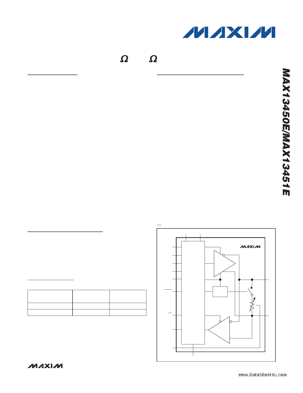
Functional Diagram (MAX13451E)
VL VCC
SRL
INV
DI
FAULT
DE
TERM
RE
RO
LOGIC-LEVEL
TRANSLATION
D
LOGIC
MAX13451E
B
A
TERM100
GND
________________________________________________________________ Maxim Integrated Products 1
For pricing, delivery, and ordering information, please contact Maxim Direct at 1-888-629-4642,
or visit Maxim’s website at www.maxim-ic.com.
1 page 
www.DataSheet4U.com
RS-485 Transceivers with Integrated
100Ω/120Ω Termination Resistors
SWITCHING CHARACTERISTICS—SRL = LOW
(VCC = +4.5V to +5.5V, VL = +1.62V to 4.2V, TA = TMIN to TMAX, unless otherwise noted. Typical values are at VCC = +5V,
VL = +1.8V, and TA = +25NC.) (Note 2)
PARAMETER
SYMBOL
CONDITIONS
MIN TYP MAX UNITS
DRIVER
Driver Propagation Delay
tDPLH
tDPHL
RDIFF = 54I, CL = 50pF, Figures 2 and 3
50
50
ns
Differential Driver Output Skew
|tDPLH - tDPHL|
tDSKEW RDIFF = 54I, CL = 50pF, Figure 3
6 ns
Driver Differential Output Rise or
Fall Time
tHL, tLH RDIFF = 54I, CL = 50pF, Figures 2 and 3
15 ns
Maximum Data Rate
Driver Enable from Shutdown to
Output High
DRMAX
tDZH(SHDN)
S2 closed, RL = 500I, CL = 100pF,
Figures 4 and 5
20
2000
Mbps
ns
Driver Enable from Shutdown to
Output Low
tDZL(SHDN)
S1 closed, RL = 500I, CL = 100pF,
Figures 4 and 5
2000
ns
Driver Disable Delay
Driver Enable Delay
RECEIVER
Receiver Propagation Delay
Receiver Output Skew
Maximum Data Rate
Receiver Enable to Output High
tDLZ, tDHZ Figures 4 and 5
tDZL, tDZH Figures 4 and 5
tRPLH
tRPHL
tRSKEW
DRMAX
tRZH
CL = 15pF, |VID| R 2.0V; tLH, tHL P 15ns,
Figures 6 and 7
CL = 15pF, Figures 6 and 7
S2 closed, CL = 100pF, RL = 500I,
Figures 8 and 9
20
100 ns
100 ns
50
50
ns
6 ns
Mbps
50 ns
Receiver Enable to Output Low
tRZL
S1 closed, CL = 100pF, RL = 500I,
Figures 8 and 9
50 ns
Receiver Disable Time from High
Receiver Disable Time from Low
Receiver Enable from Shutdown
to Output High
tRHZ
tRLZ
tRZH(SHDN)
Figures 8 and 9
Figures 8 and 9
Figures 8 and 9
50
50
2000
ns
ns
ns
Receiver Enable from Shutdown
to Output Low
tRZL(SHDN) Figures 8 and 9
2000
ns
TERMINATION RESISTOR
Turn-Off Time
Turn-On Time
tRTZ
tRTEN
Figure 10
Figure 10
120 Fs
1 Fs
Note 2: All devices are 100% production tested at TA = +25°C. Limits over temperature are guaranteed by design.
Note 3: Termination resistance is disabled (TERM = high).
_______________________________________________________________________________________ 5
5 Page 
www.DataSheet4U.com
TOP VIEW
DE
RE
DI
VCC
TERM
VL
RO
1
2
3
4
5
6
7
RS-485 Transceivers with Integrated
100Ω/120Ω Termination Resistors
Pin Configurations
MAX13450E
EP
TSSOP
14 SRL
13 TERM100
12 Z
11 GND
10 Y
9B
8A
TOP VIEW
DE
RE
DI
VCC
TERM
VL
RO
1
2
3
4
5
6
7
MAX13451E
EP
TSSOP
14 SRL
13 TERM100
12 B
11 GND
10 A
9 FAULT
8 INV
PIN
MAX13450E MAX13451E
11
22
33
44
55
66
7—
—7
8—
— 10
9—
— 12
NAME
DE
RE
DI
VCC
TERM
VL
RO
RO
A
A
B
B
Pin Description
FUNCTION
Driver-Output Enable. Drive DE low to put the driver output in three-state. Drive DE
high to enable the driver. DE is referenced to VL.
Receiver-Output Enable. Drive RE low to enable the RO. Drive RE high to disable
the RO output and put the RO output in a high-impedance state. RE is referenced
to VL.
Driver Input. Drive DI low to force the noninverting output low and the inverting
output high. Drive DI high to force the noninverting output high and inverting out-
put low. DI is referenced to VL.
Power-Supply Voltage. Bypass VCC to GND with a 0.1FF ceramic capacitor
placed as close as possible to the device.
Active-Low Termination Resistor Enable. Drive TERM low to enable the internal ter-
mination resistor. TERM is referenced to VL.
Logic Supply Voltage. Bypass VL to GND with a 0.1FF ceramic capacitor placed
as close as possible to the device.
Receiver Output. When receiver is enabled and VA - VB R -50mV, RO is high. If
VA - VB P -200mV, RO is low. RO is referenced to VL.
Receiver Output. When INV is low, receiver is enabled and VA - VB R -50mV, RO is
high. If VA - VB P -200mV, RO is low. When INV is high, receiver is enabled and
VA - VB R -50mV, RO is low. If VA - VB P -200mV, RO is high. RO is referenced to VL.
Noninverting Receiver Input
If INV is low, A is a noninverting receiver input and a noninverting driver output. If
INV is high, A is an inverting receiver input and an inverting driver output.
Inverting Receiver Input
If INV is low, B is an inverting receiver input and an inverting driver output. If INV
is high, B is a noninverting receiver input and a noninverting driver output.
______________________________________________________________________________________ 11
11 Page | ||
| Páginas | Total 17 Páginas | |
| PDF Descargar | [ Datasheet MAX13451E.PDF ] | |
Hoja de datos destacado
| Número de pieza | Descripción | Fabricantes |
| MAX13451E | RS-485 Transceivers | Maxim Integrated Products |
| Número de pieza | Descripción | Fabricantes |
| SLA6805M | High Voltage 3 phase Motor Driver IC. |
Sanken |
| SDC1742 | 12- and 14-Bit Hybrid Synchro / Resolver-to-Digital Converters. |
Analog Devices |
|
DataSheet.es es una pagina web que funciona como un repositorio de manuales o hoja de datos de muchos de los productos más populares, |
| DataSheet.es | 2020 | Privacy Policy | Contacto | Buscar |