|
|
|
PDF RC32365 Data sheet ( Hoja de datos )
| Número de pieza | RC32365 | |
| Descripción | IDT Interprise Integrated Communications Processor | |
| Fabricantes | Integrated Device Technology | |
| Logotipo | ||
Hay una vista previa y un enlace de descarga de RC32365 (archivo pdf) en la parte inferior de esta página. Total 30 Páginas | ||
|
No Preview Available !
IDTTM InterpriseTM Integrated
Communications Processor
www.DRatCaS3he2et34U6.c5om
Device Overview
The RC32365 device is a member of the IDT™ Interprise™ family of
integrated communications processors. This device is designed to
address a range of communications applications that require the effi-
cient processing of IPSec algorithms. These applications include gate-
ways, wireless access points, and virtual private network (VPN)
equipment. The key to the RC32365’s efficient processing of IPSec
algorithms is a highly progammable security engine which off-loads the
CPU core of encryption/decryption, hashing, and padding tasks.
Features List
x RC32300 32-bit CPU core
– 32-bit MIPS instruction set
– Supports big or little endian operation
– MMU
– 16-entry TLB
– Supports variable page sizes and enhanced write algo-
rit hm
– Supports variable number of locked entries
– 8KB Instruction Cache
– 2-way set associative
– LRU replacement algorithm
– 4 word line size
– Sub-block ordering
– Word parity
– Per line cache locking
– 2KB Data Cache
– 2-way set associative
– LRU replacement algorithm
– 4 word line size
– Sub-block ordering
– Byte parity
– Per line cache locking
– Can be programmed on a page basis to implement write-
through no write allocate, write-through write al ocate, or
write-back algorithms
– Enhanced EJTAG and JTAG Interfaces
– Compatible with IEEE Std. 1149.1-1990
x Security Engine
– Dedicated DMA channels for high speed data transfers to and
from the security engine
– On-chip memory for storage of two security contexts
– Supports ECB and CBC modes for the following symmetric
encryption algorithms: DES, triple DES (both two key (k1=k3)
and three key (k1!=k3) modes), AES-128 with 128-bit blocks,
AES-192 with 128-bit blocks
– Hardware support for encryption pad generation and checking
using one of seven popular padding algorithms: supports pad
algorithm required by IPSec ESP
– Supports MD5 and SHA-1 one-way hash functions
– Programmable truncation length of computed hash and HMAC
on a security context basis
– Supports concurrent hash and encryption operations
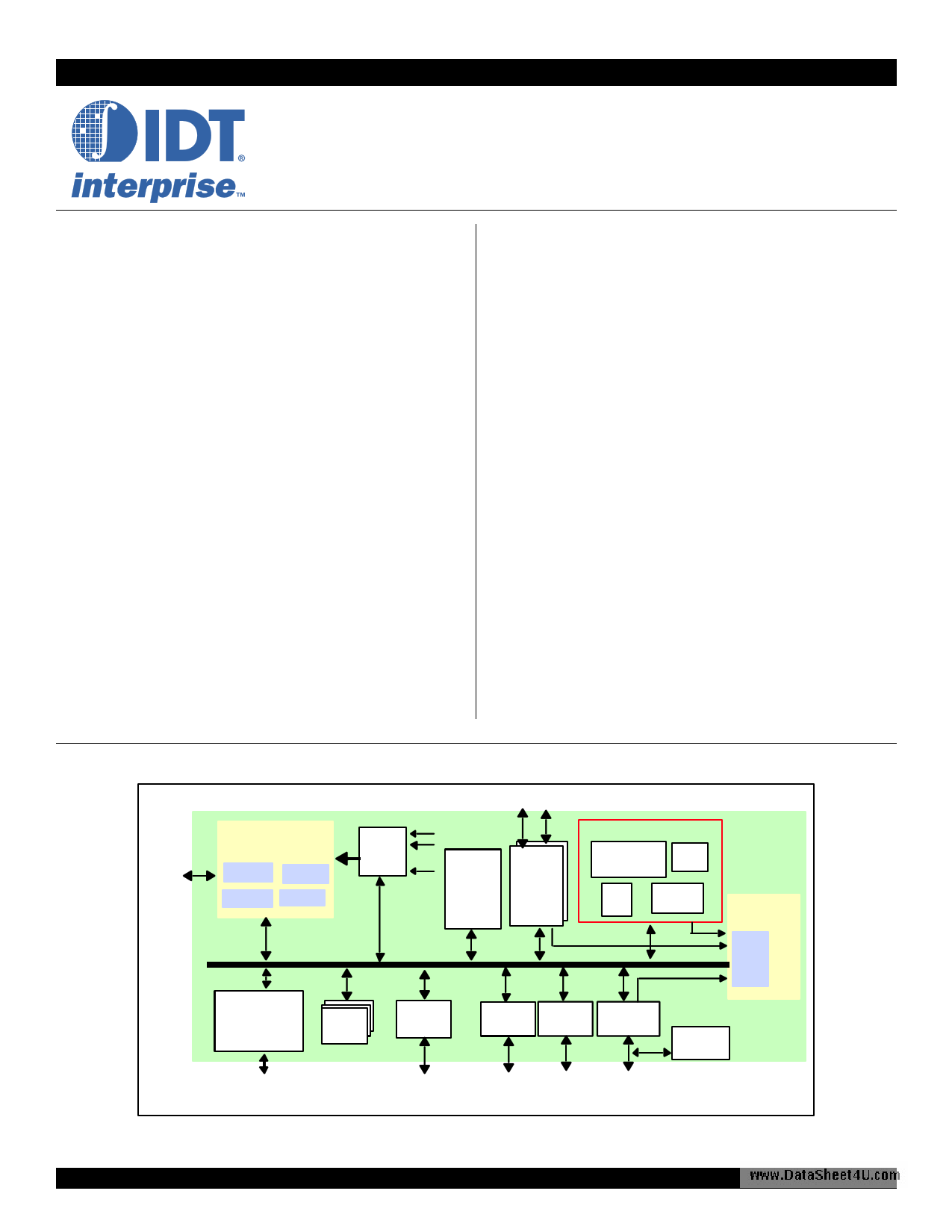
Block Diagram
JTAG
32-bitMIPS
CPUCore
EJTAG
D. Cache
MMU
I. Cache
MII MII
Interrupt
Controller
.
.
Bus/System
Integrity
Moni tor
2 Ethernet
10/100
Interfaces
SecurityFunctions
Security
Context Storage
RNG
Hash
Unit
Encryption
Unit
DMA
Controll er
IPBusTM
Arbiter
SDRAM &Device
Controllers
including PCMCIA
Support
3Counter
Timers
UART
(16550)
GPIO
Interface
SPI
Control ler
PCI
Master/Target
Interface
PCI Arbiter
(Host Mode)
Memory &
Peripheral Bus
(i ncludi ngPCMCIA)
Serial Channel
GPIO Pins SPI Bus
PCI Bus
Figure 1 RC32365 Internal Block Diagram
20 03 Integrated Device Techno logy, In c.
IDT and the IDT logo are registered trademarks of Integrated Device Technology, Inc.
1 of 44
February 25, 2004
DSC 6210
1 page 
RC32365
Signal
Type
Name/Description
General Purpose I/O
GPIO[0]
I/O
GPIO[1]
I/O
GPIO[2]
I/O
GPIO[3]
I/O
GPIO[4]
I/O
GPIO[5]
I/O
GPIO[6]
GPIO[7]
I/O
I/O
GPIO[8]
GPIO[9]
GPIO[10]
GPIO[11]
GPIO[12]
GPIO[13]
GPIO[14]
I/O
I/O
I/O
I/O
I/O
I/O
I/O
General Purpose I/O. This pin can be configured as a general purpose I /O pin.
Alternate function pin name: U0SOUT
Alternate function: UART channel 0 serial output .
General Purpose I/O. This pin can be configured as a general purpose I /O pin.
Alternate function pin name: U0SINP
Alternate function: UART channel 0 serial input.
General Purpose I/O. This pin can be configured as a general purpose I /O pin.
Alternate function pin name: MADDR[22]
Alternate function: Memory and Peripheral bus address bit 22 (output).
General Purpose I/O. This pin can be configured as a general purpose I /O pin.
Alternate function pin name: MADDR[23]
Alternate function: Memory and Peripheral bus address bit 23 (output).
General Purpose I/O. This pin can be configured as a general purpose I /O pin.
Alternate function pin name: MADDR[24]
Alternate function: Memory and Peripheral bus address bit 24 (output).
General Purpose I/O. This pin can be configured as a general purpose I /O pin.
Alternate function pin name: MADDR[25]
Alternate function: Memory and Peripheral bus address bit 25 (output).
General Purpose I/O. This pin can be configured as a general purpose I /O pin.
The value of this pin may be used as a Counter Timer Clock input.
General Purpose I/O. This pin can be configured as a general purpose I /O pin.
Alternate function pin name: SDCKENP
Alternate function: SDRAM clock enable output
The value of this pin may be used as a Counter Timer Clock input.
General Purpose I/O. This pin can be configured as a general purpose I /O pin.
Alternate function pin name: CEN1
Alternate function: PCMCIA chip enable 1 (CE1#) (output).
General Purpose I/O. This pin can be configured as a general purpose I /O pin.
Alternate function pin name: CEN2
Alternate function: PCMCIA chip enable 2 (CE2#) (output).
General Purpose I/O. This pin can be configured as a general purpose I /O pin.
Alternate function pin name: REGN
Alternate function: PCMCIA Attribute Memory Select (REG#) (output).
General Purpose I/O. This pin can be configured as a general purpose I /O pin.
Alternate function pin name: IORDN
Alternate function: PCMCIA IO Read (IORD#) (output).
General Purpose I/O. This pin can be configured as a general purpose I /O pin.
Alternate function pin name: IOWRN
Alternate function: PCMCIA IO Write (IOWR#) (output).
General Purpose I/O. This pin can be configured as a general purpose I /O pin.
Alternate function pin name: PCIREQN[2]
Alternate function: PCI bus request 2 (output).
General Purpose I/O. This pin can be configured as a general purpose I /O pin.
Alternate function pin name: PCIGNTN[2]
Alternate function: PCI bus grant 2 (output).
Tabl e 1 Pin Description (Part 2 of 6)
www.DataSheet4U.com
5 of 44
February 25, 2004
5 Page 
RC32365
Boot Configuration Vector
www.DataSheet4U.com
The boot configuration vector is read into the RC32365 during cold reset. The vector defines parameters in the RC32365 that are essential to oper-
ation when cold reset is complete.
The encoding of boot configuration vector is described in Table 3, and the vector input is illustrated in Figure 4.
Signal
MD ATA[2:0]
MD ATA[3]
MD ATA[4]
MD ATA[6:5]
MD ATA[7]
MD ATA[8]
MD ATA[11:9]
MD ATA[15:12]
Name/Description
CPU Clock Multiplier. This field specifies the value by which the PLL multiplies the master
clock input (CLK) to obtain the processor clock frequency (PCLK).
0x0 - Multiply by 2
0x1 - 0x7 — Reserved
Endian. This bit specifies the endianness.
0x0 - little endian
0x1 - big endian
Reserved. This pin may be driven high or low during boot configuration and its state is
recorded in the Boot Configuration Vector (BCV) field of the BCV register. This reserved bit
may be used to pass boot configuration parameters to software.
Boot Device Width. This field specifies the width of the boot device (i.e., Device 0).
0x0 - 8-bit boot device width
0x1 - 16-bit boot device width
0x2 - 32-bit boot device width
0x3 - reserved
Reset Mode. This bit specifies the length of time the RSTN signal is driven.
0x0 - Normal reset: RSTN driven for minimum of 4096 clock cycles
0x1 - reserved
Disabl e Watchdog Timer. When this bit is set, the watchdog timer is disabled following a cold
reset.
0x0 - Watchdog timer is enabled
0x1 - Watchdog timer is disabled
PCI Mode. This bit controls the operating mode of the PCI bus interface. The initial value of the
EN bit in the PCIC register is determined by the PCI mode.
0x0 - Disabled (EN initial value is zero)
0x1 - PCI satellite mode with PCI target not ready (EN initial value is one)
0x2 - PCI satellite mode with suspended CPU execution (EN initial value is one)
0x3 - PCI host mode with external arbiter (EN initial value is zero)
0x4 - PCI host mode with int ernal arbiter using fixed priority arbitration algorithm
(EN init ial value is zero)
0x5 - PCI host mode with int ernal arbiter using round robin arbitration algorithm
(EN init ial value is zero)
0x6 - reserved
0x7 - reserved
Reserved. These pins may be driven high or low during boot configuration and their state is
recorded in the Boot Configuration Vector (BCV) field of the BCV register. These reserved bits
may be used to pass boot configuration parameters to software.
Table 3 Boot Configuration Vector Encoding
11 of 44
February 25, 2004
11 Page | ||
| Páginas | Total 30 Páginas | |
| PDF Descargar | [ Datasheet RC32365.PDF ] | |
Hoja de datos destacado
| Número de pieza | Descripción | Fabricantes |
| RC32365 | IDT Interprise Integrated Communications Processor | Integrated Device Technology |
| Número de pieza | Descripción | Fabricantes |
| SLA6805M | High Voltage 3 phase Motor Driver IC. |
Sanken |
| SDC1742 | 12- and 14-Bit Hybrid Synchro / Resolver-to-Digital Converters. |
Analog Devices |
|
DataSheet.es es una pagina web que funciona como un repositorio de manuales o hoja de datos de muchos de los productos más populares, |
| DataSheet.es | 2020 | Privacy Policy | Contacto | Buscar |