|
|
|
PDF ICS8737I-11 Data sheet ( Hoja de datos )
| Número de pieza | ICS8737I-11 | |
| Descripción | DIFFERENTIAL-TO- 3.3V LVPECL CLOCK GENERATOR | |
| Fabricantes | Integrated Circuit Systems | |
| Logotipo | ||
Hay una vista previa y un enlace de descarga de ICS8737I-11 (archivo pdf) en la parte inferior de esta página. Total 14 Páginas | ||
|
No Preview Available !
Integrated
Circuit
Systems, Inc.
ICS8737I-11
L S ¸1/¸2OW wKwEwW.DataSheet4U.com
DIFFERENTIAL-TO- 3.3V LVPECL CLOCK GENERATOR
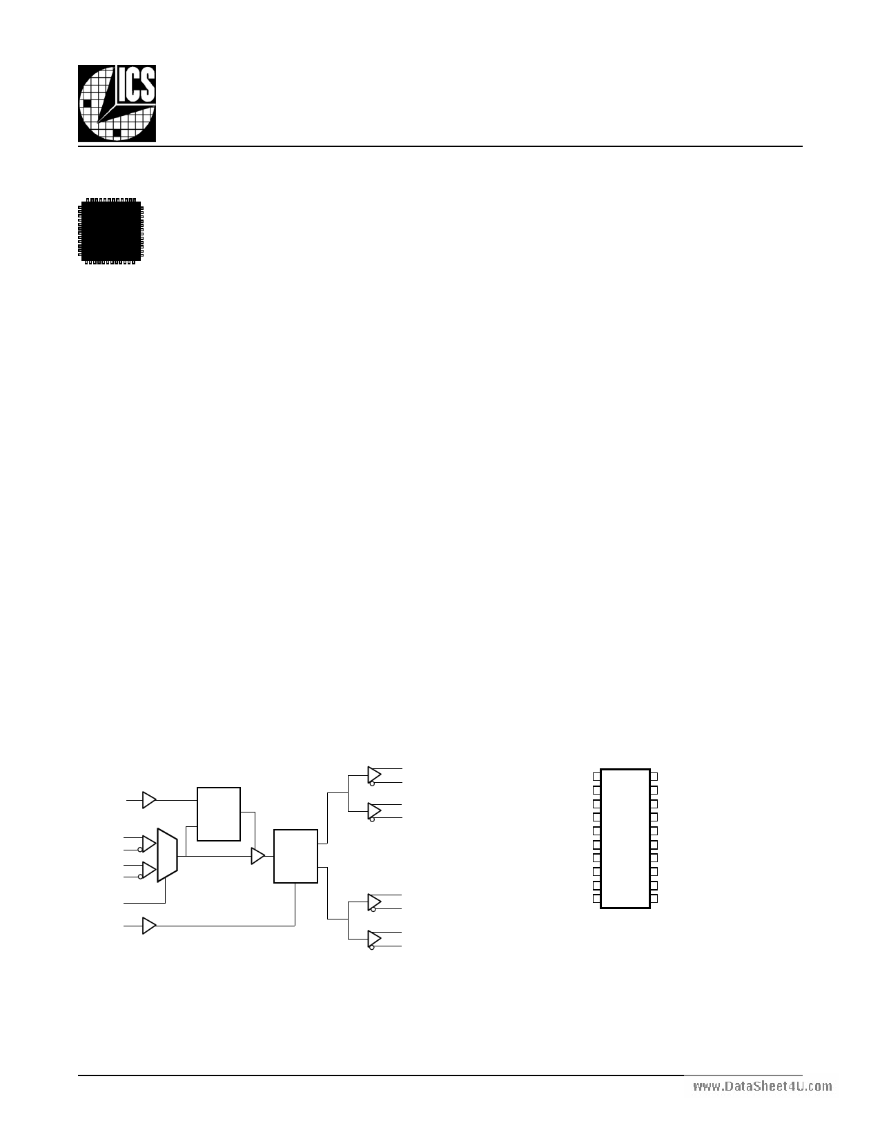
GENERAL DESCRIPTION
The ICS8737I-11 is a low skew, high perfor-
,&6 mance Differential-to-3.3V LVPECL Clock
HiPerClockS™ G e n e r a t o r / D i v i d e r a n d a m e m b e r o f t h e
HiPerClockS™ family of High Performance Clock
Solutions from ICS. The ICS8737I-11 has two
selectable clock inputs. The CLK, nCLK pair can accept most
standard differential input levels. The PCLK, nPCLK pair can
accept LVPECL, CML, or SSTL input levels.The clock
enable is internally synchronized to eliminate runt pulses
on the outputs during asynchronous assertion/deassertion
of the clock enable pin.
Guaranteed output and part-to-part skew characteristics
make the ICS8737I-11 ideal for clock distribution applications
demanding well defined performance and repeatability.
FEATURES
• 2 divide by 1 differential 3.3V LVPECL outputs;
2 divide by 2 differential 3.3V LVPECL outputs
• Selectable differential CLK, nCLK or LVPECL clock inputs
• CLK, nCLK pair can accept the following differential
input levels: LVDS, LVPECL, LVHSTL, SSTL, HCSL
• PCLK, nPCLK supports the following input types:
LVPECL, CML, SSTL
• Maximum output frequency: 650MHz
• Translates any single ended input signal (LVCMOS, LVTTL,
GTL) to LVPECL levels with resistor bias on nCLK input
• Output skew: 75ps (maximum)
• Part-to-part skew: 300ps (maximum)
• Bank skew: Bank A - 30ps (maximum)
Bank B - 45ps (maximum)
• 3.3V operating supply
• -40°C to 85°C ambient operating temperature
BLOCK DIAGRAM
CLK_EN
CLK
nCLK
PCLK
nPCLK
CLK_SEL
MR
D
Q
LE
0
1
÷1
÷2
PIN ASSIGNMENT
QA0
nQA0
QA1
nQA1
QB0
nQB0
QB1
nQB1
VEE 1
20 QA0
CLK_EN 2 19 nQA0
CLK_SEL 3 18 VCC
CLK 4 17 QA1
nCLK 5 16 nQA1
PCLK 6 15 QB0
nPCLK 7 14 nQB0
nc 8
13 VCC
MR 9 12 QB1
VCC 10 11 nQB1
ICS8737I-11
20-Lead TSSOP
6.50mm x 4.40mm x 0.92 package body
G Package
Top View
8737AGI-11
www.icst.com/products/hiperclocks.html
1
REV. A JUNE 3, 2002
1 page 
Integrated
Circuit
Systems, Inc.
ICS8737I-11
L S ¸1/¸2OW wKwEwW.DataSheet4U.com
DIFFERENTIAL-TO- 3.3V LVPECL CLOCK GENERATOR
TABLE 4D. LVPECL DC CHARACTERISTICS, VCC = 3.3V±5%, TA = -40°C TO 85°C
Symbol Parameter
Test Conditions
Minimum Typical
I Input High Current
IH
VIN = VCC = 3.465V
VIN = VCC = 3.465V
IIL Input Low Current
VIN = 0V, VCC = 3.465V
V = 0V, V = 3.465V
IN CC
-5
-150
VPP Peak-to-Peak Input Voltage
0.3
VCMR
Common Mode Input Voltage; NOTE 1, 2
VEE + 1.5
VOH Output High Voltage; NOTE 3
VCC - 1.4
VOL Output Low Voltage; NOTE 3
VCC - 2.0
VSWING Peak-to-Peak Output Voltage Swing
0.6
NOTE 1: Common mode voltage is defined as VIH.
NOTE 2: For single ended applications, the maximum input voltage for PCLK, nPCLK is VCC + 0.3V.
NOTE 3: Outputs terminated with 50Ω to VCC - 2V.
Maximum
150
5
1
VCC
VCC - 1.0
VCC - 1.7
0.9
Units
µA
µA
µA
µA
V
V
V
V
V
TABLE 5. AC CHARACTERISTICS, VCC = 3.3V±5%, TA = -40°C TO 85°C
Symbol Parameter
Test Conditions Minimum Typical Maximum
fMAX Output Frequency
CLK, nCLK
tPD
Propagation Delay; NOTE 1
PCLK, nPCLK
IJ 650MHz
IJ 650MHz
1.2
1.1
650
1.8
1.7
tsk(o) Output Skew; NOTE 2, 4
75
tsk(b) Bank Skew; NOTE 4
Bank A
Bank B
30
45
tsk(pp) Part-to-Part Skew; NOTE 3, 4
300
tR Output Rise Time
tF Output Fall Time
odc Output Duty Cycle
20% to 80% @ 50MHz 300
700
20% to 80% @ 50MHz 300
700
47 50 53
All parameters measured at 500MHz unless noted otherwise.
The cycle-to-cycle jitter on the input will equal the jitter on the output. The part does not add jitter.
NOTE 1: Measured from the differential input crossing point to the differential output crossing point.
NOTE 2: Defined as skew between outputs at the same supply voltage and with equal load conditions.
Measured at the output differential cross points.
NOTE 3: Defined as skew between outputs on different devices operating at the same supply voltages
and with equal load conditions. Using the same type of inputs on each device, the outputs are measured
at the differential cross points.
NOTE 4: This parameter is defined in accordance with JEDEC Standard 65.
Units
MHz
ns
ns
ps
ps
ps
ps
ps
ps
%
8737AGI-11
www.icst.com/products/hiperclocks.html
5
REV. A JUNE 3, 2002
5 Page 
Integrated
Circuit
Systems, Inc.
ICS8737I-11
L S ¸1/¸2OW wKwEwW.DataSheet4U.com
DIFFERENTIAL-TO- 3.3V LVPECL CLOCK GENERATOR
RELIABILITY INFORMATION
TABLE 7. θJAVS. AIR FLOW TABLE
q by Velocity (Linear Feet per Minute)
JA
Single-Layer PCB, JEDEC Standard Test Boards
Multi-Layer PCB, JEDEC Standard Test Boards
0
114.5°C/W
73.2°C/W
200
98.0°C/W
66.6°C/W
500
88.0°C/W
63.5°C/W
NOTE: Most modern PCB designs use multi-layered boards. The data in the second row pertains to most designs.
TRANSISTOR COUNT
The transistor count for ICS8737I-11 is: 510
8737AGI-11
www.icst.com/products/hiperclocks.html
11
REV. A JUNE 3, 2002
11 Page | ||
| Páginas | Total 14 Páginas | |
| PDF Descargar | [ Datasheet ICS8737I-11.PDF ] | |
Hoja de datos destacado
| Número de pieza | Descripción | Fabricantes |
| ICS8737I-11 | DIFFERENTIAL-TO- 3.3V LVPECL CLOCK GENERATOR | Integrated Circuit Systems |
| Número de pieza | Descripción | Fabricantes |
| SLA6805M | High Voltage 3 phase Motor Driver IC. |
Sanken |
| SDC1742 | 12- and 14-Bit Hybrid Synchro / Resolver-to-Digital Converters. |
Analog Devices |
|
DataSheet.es es una pagina web que funciona como un repositorio de manuales o hoja de datos de muchos de los productos más populares, |
| DataSheet.es | 2020 | Privacy Policy | Contacto | Buscar |