|
|
|
PDF K4X1G163PC-FE Data sheet ( Hoja de datos )
| Número de pieza | K4X1G163PC-FE | |
| Descripción | Mobile DDR SDRAM | |
| Fabricantes | Samsung semiconductor | |
| Logotipo | ||
Hay una vista previa y un enlace de descarga de K4X1G163PC-FE (archivo pdf) en la parte inferior de esta página. Total 20 Páginas | ||
|
No Preview Available !
K4X1G163PC - L(F)E/G
Mobile DDR SDRAM
64Mx16 Mobile DDR SDRAM
1. FEATURES
• VDD/VDDQ = 1.8V/1.8V
• Double-data-rate architecture; two data transfers per clock cycle
• Bidirectional data strobe(DQS)
• Four banks operation
• Differential clock inputs(CK and CK)
• MRS cycle with address key programs
- CAS Latency ( 3 )
- Burst Length ( 2, 4, 8, 16 )
- Burst Type (Sequential & Interleave)
• EMRS cycle with address key programs
- Partial Array Self Refresh ( Full, 1/2, 1/4 Array )
- Output Driver Strength Control ( Full, 1/2, 1/4, 1/8 )
• Internal Temperature Compensated Self Refresh
• All inputs except data & DM are sampled at the positive going edge of the system clock(CK).
www.Da• DtaaStaheI/eOt4trUa.ncsoamctions on both edges of data strobe, DM for masking.
• Edge aligned data output, center aligned data input.
• No DLL; CK to DQS is not synchronized.
• LMD, UMD for write masking only.
• Auto refresh duty cycle
- 7.8us for -25 to 85 °C
2. Operating Frequency
Speed @CL21)
Speed @CL31)
NOTE:
1) CAS Latency
3. Address configuration
DDR333
83Mhz
166Mhz
DDR266
83Mhz
133Mhz
Organization
64Mx16
- DM is internally loaded to match DQ and DQS identically.
4. Ordering Information
Bank Address
BA0,BA1
Row Address
A0 - A13
Column Address
A0 - A9
Part No.
K4X1G163PC-L(F)E/GC6
K4X1G163PC-L(F)E/GC3
Max Freq.
166MHz(CL=3),83MHz(CL=2)
133MHz(CL=3),83MHz(CL=2)
- L(F)E : 60FBGA Pb(Pb Free), Normal Power, Extended Temperature(-25 °C ~ 85 °C)
- L(F)G : 60FBGA Pb(Pb Free), Low Power, Extended Temperature(-25 °C ~ 85 °C)
- C6/C3 : 166MHz(CL=3) / 133MHz(CL=3)
Interface
LVCMOS
Package
60FBGA
Pb (Pb Free)
INFORMATION IN THIS DOCUMENT IS PROVIDED IN RELATION TO SAMSUNG PRODUCTS, AND IS SUBJECT TO CHANGE WITHOUT NOTICE. NOTH-
ING IN THIS DOCUMENT SHALL BE CONSTRUED AS GRANTING ANY LICENSE, EXPRESS OR IMPLIED, BY ESTOPPEL OR OTHERWISE, TO ANY
INTELLECTUAL PROPERTY RIGHTS IN SAMSUNG PRODUCTS OR TECHNOLOGY. ALL INFORMATION IN THIS DOCUMENT IS PROVIDED ON AS "AS IS"
BASIS WITHOUT GUARANTEE OR WARRANTY OF ANY KIND.
1. For updates or additional information about Samsung products, contact your nearest Samsung office.
2. Samsung products are not intended for use in life support, critical care, medical, safety equipment, or similar applications where Product failure could result in
loss of life or personal or physical harm, or any military or defense application, or any governmental procurement to which special terms or provisions may apply.
- 4 - November 2007
1 page 
K4X1G163PC - L(F)E/G
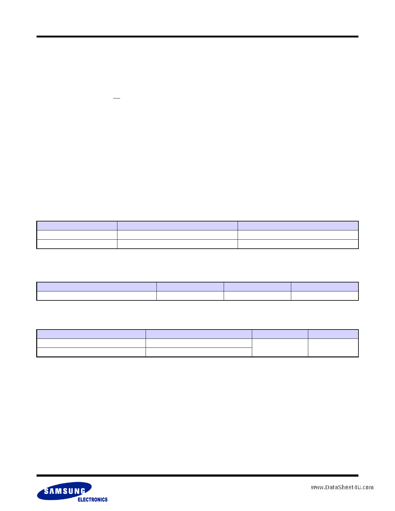
8. Functional Description
POWER
APPLIED
POWER
ON
PRECHARGE
ALL BANKS
www.DataSheet4U.com
EMRS
MRS
Mobile DDR SDRAM
Figure 1. State diagram
CKEH
MRS
DEEP
POWER
DOWN
PARTIAL
SELF
REFRESH SELF
DEEP
REFRESH
POWER
DOWN
REFS
IDLE
ALL BANKS
PRECHARGED
REFSX
REFA
CKEL
AUTO
REFRESH
CKEH
ACT
POWER
DOWN
POWER
DOWN
CKEH
CKEL
WRITE
ROW
ACTIVE
BURST STOP
READ
WRITEA
WRITE
WRITEA READA
READ
READ
WRITEA
WRITEA
READA
PRE
PRE
PRE
READA
READA
PRE
PRECHARGE
PREALL
Automatic Sequence
Command Sequence
- 8 - November 2007
5 Page 
K4X1G163PC - L(F)E/G
Mobile DDR SDRAM
12. DC CHARACTERISTICS
Recommended operating conditions (Voltage referenced to VSS = 0V, Tc = -25 to 85°C)
Parameter
Symbol
Test Condition
DDR333 DDR266 Unit Note
Operating Current
(One Bank Active)
IDD0 tRC=tRCmin; tCK=tCKmin; CKE is HIGH; CS is HIGH between valid commands;
address inputs are SWITCHING; data bus inputs are STABLE
100
90 mA
Precharge Standby Current
in power-down mode
IDD2P
IDD2PS
all banks idle, CKE is LOW; CS is HIGH, tCK = tCKmin;
address and control inputs are SWITCHING; data bus inputs are STABLE
all banks idle, CKE is LOW; CS is HIGH, CK = LOW, CK = HIGH;
address and control inputs are SWITCHING; data bus inputs are STABLE
0.5
mA
0.5
Precharge Standby Current
in non power-down mode
IDD2N
all banks idle, CKE is HIGH; CS is HIGH, tCK = tCKmin;
address and control inputs are SWITCHING; data bus inputs are STABLE
IDD2NS
all banks idle, CKE is HIGH; CS is HIGH, CK = LOW, CK = HIGH;
address and control inputs are SWITCHING; data bus inputs are STABLE
15 12
mA
88
Active Standby Current
www.DaintapoSwheer-edto4wUn.cmoomde
IDD3P
one bank active, CKE is LOW; CS is HIGH, tCK = tCKmin;
address and control inputs are SWITCHING; data bus inputs are STABLE
IDD3PS
one bank active, CKE is LOW; CS is HIGH, CK = LOW, CK = HIGH;
address and control inputs are SWITCHING; data bus inputs are STABLE
5
mA
3
Active Standby Current
in non power-down mode
(One Bank Active)
IDD3N
one bank active, CKE is HIGH; CS is HIGH, tCK = tCKmin;
address and control inputs are SWITCHING; data bus inputs are STABLE
IDD3NS one bank active, CKE is HIGH; CS is HIGH, CK = LOW, CK = HIGH;
address and control inputs are SWITCHING; data bus inputs are STABLE
25 25
mA
20 20
Operating Current
(Burst Mode)
IDD4R one bank active; BL=4; CL=3; tCK = tCKmin; continuous read bursts; I OUT =0 mA
address inputs are SWITCHING; 50% data change each burst transfer
IDD4W one bank active; BL = 4; tCK = tCKmin ; continuous write bursts;
address inputs are SWITCHING; 50% data change each burst transfer
150
130
135
mA
115
Refresh Current
IDD5
tRC = tRFCmin ; tCK = tCKmin ; burst refresh; CKE is HIGH;
address and control inputs are SWITCHING; data bus inputs are STABLE
CKE is LOW; t CK = t CKmin ;
Extended Mode Register set to all 0’s;
address and control inputs are STABLE;
data bus inputs are STABLE
Parameter
Full Array
- E 1/2 Array
200
451)
600
500
180
85
1200
900
mA
°C
Self Refresh Current
IDD6
1/4 Array
Full Array
450
500
750
1000
uA
-G
1/2 Array 440
800
1/4 Array 400
700
Deep Power Down Current IDD8 Deep Power Down Mode Current
25 uA 2
NOTE :
1) It has +/- 5°C tolerance.
2) DPD(Deep Power Down) function is an optional feature, and it will be enabled upon request.
Please contact Samsung for more information.
3) IDD specifications are tested after the device is properly intialized.
4) Input slew rate is 1V/ns.
5) Definitions for IDD: LOW is defined as V IN ≤ 0.1 * VDDQ ;
HIGH is defined as V IN ≥ 0.9 * VDDQ ;
STABLE is defined as inputs stable at a HIGH or LOW level ;
SWITCHING is defined as: - address and command: inputs changing between HIGH and LOW once per two clock cycles ;
- data bus inputs: DQ changing between HIGH and LOW once per clock cycle; DM and DQS are STABLE.
- 14 -
November 2007
11 Page | ||
| Páginas | Total 20 Páginas | |
| PDF Descargar | [ Datasheet K4X1G163PC-FE.PDF ] | |
Hoja de datos destacado
| Número de pieza | Descripción | Fabricantes |
| K4X1G163PC-FE | Mobile DDR SDRAM | Samsung semiconductor |
| K4X1G163PC-FG | Mobile DDR SDRAM | Samsung semiconductor |
| Número de pieza | Descripción | Fabricantes |
| SLA6805M | High Voltage 3 phase Motor Driver IC. |
Sanken |
| SDC1742 | 12- and 14-Bit Hybrid Synchro / Resolver-to-Digital Converters. |
Analog Devices |
|
DataSheet.es es una pagina web que funciona como un repositorio de manuales o hoja de datos de muchos de los productos más populares, |
| DataSheet.es | 2020 | Privacy Policy | Contacto | Buscar |