|
|
|
PDF PE9354 Data sheet ( Hoja de datos )
| Número de pieza | PE9354 | |
| Descripción | SPDT High Power UltraCMOS RF Switch Rad hard for Space Applications | |
| Fabricantes | Peregrine Semiconductor | |
| Logotipo | ||
Hay una vista previa y un enlace de descarga de PE9354 (archivo pdf) en la parte inferior de esta página. Total 7 Páginas | ||
|
No Preview Available !
Product Description
The PE9354 SPDT High Power UltraCMOS™ RF Switch is
designed to cover a broad range of applications from near DC
to 3000 MHz. This single-supply reflective switch integrates on-
board CMOS control logic driven by a simple, single-pin CMOS
and TTL compatible control input. Using a nominal +3-volt
power supply, a typical input 1 dB compression point of +31
dBm can be achieved. The PE9354 also exhibits input-output
isolation of better than 30 dB at 2000 MHz and is offered in a
small 8-lead ceramic SOIC package.
The PE9354 is optimized for commercial space applications.
Single Event Latch up (SEL) is physically impossible and
Single Event Upset (SEU) is better than 10-9 errors per bit/day.
Fabricated in Peregrine’s UltraCMOS™ technology, the
PE9354 offers excellent RF performance and intrinsic radiation
tolerance.
Product Swpwwe.DcatiafSihceeat4tUi.oconm
PE9354
SPDT High Power
UltraCMOS™ RF Switch
Rad hard for Space Applications
Features
• Single 3-volt power supply
• Low insertion loss: 0.55 dB at 2000 MHz
• High isolation of 30 dB at 2000 MHz
• Typical input 1 dB compression point of
+31 dBm
• 100 Krad total dose
• Single-pin CMOS or TTL logic control
• Low cost
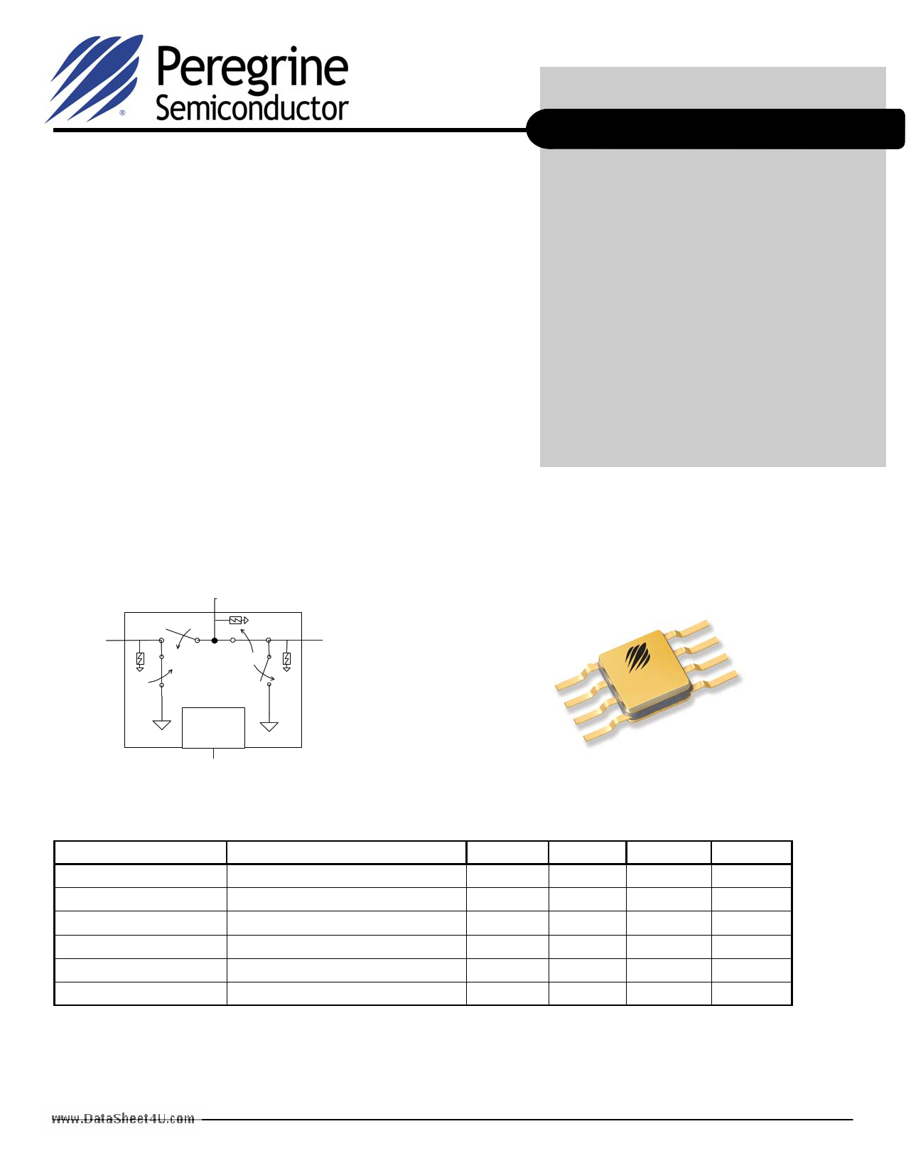
Figure 1. Functional Schematic Diagram
RFC
Figure 2. Package Type
8-lead CSOIC
RF1 RF2
CMOS
Control
Driver
CTRL
Table 1. A/C Electrical Specifications -55 °C to +125 °C, VDD = 3.0 V (ZS = ZL = 50 Ω)
Parameter
Conditions
Operation Frequency1
Insertion Loss
2000 MHz
Isolation – RFC to RF1/RF2
2000 MHz
Isolation – RF1 to RF2
2000 MHz
Return Loss2
2000 MHz
Input 1 dB Compression
2000 MHz
Note: 1. Device linearity will begin to degrade below 10 MHz.
Note: 2. Return loss not measured in production due to equipment limitations
Minimum
DC
28
24
28
Typical
0.55
32
28
22
31
Maximum
3000
0.80
Units
MHz
dB
dB
dB
dB
dBm
Document No. 70-0099-02 │ www.psemi.com
©2004-2006 Peregrine Semiconductor Corp. All rights reserved.
Page 1 of 7
1 page 
PE9354
Product Specification
Evaluation Kit Information
Evaluation Kit
The SPDT Switch Evaluation Kit board was designed to
ease customer evaluation of the PE9354 SPDT switch.
The RF common port is connected through a 50 Ω
transmission line to the top left SMA connector, J1.
Port 1 and Port 2 are connected through 50 Ω
transmission lines to the top two SMA connectors on
the right side of the board, J2 and J3. A through
transmission line connects SMA connectors J4 and J5.
This transmission line can be used to estimate the loss
of the PCB over the environmental conditions being
evaluated.
The board is constructed of a two metal layer FR4
material with a total thickness of 0.031”. The bottom
layer provides ground for the RF transmission lines.
The transmission lines were designed using a coplanar
waveguide with ground plane model using a trace width
of 0.030”, trace gaps of 0.007”, dielectric thickness of
0.028”, metal thickness of 0.0014” and εr of 4.4.
J6 provides a means for controlling DC and digital
inputs to the device. Starting from the lower left pin,
the second pin to the right (J2-3) is connected to the
device CNTL input. The fourth pin to the right (J2-7) is
connected to the device VDD input. A decoupling
capacitor (100 pF) is provided on both CTRL and VDD
traces. It is the responsibility of the customer to
determine proper supply decoupling for their design
application. Removing these components from the
evaluation board has not been shown to degrade RF
performance.
The ground plane has been removed from beneath the
device for performance issues. It was found that
insertion loss dips (suck-outs) were experienced due to
the capacitive effect of the metal package sitting
insulated by the solder-mask on the ground plane. All
www.DataSheet4U.com
Figure 12. Evaluation Board Layouts
data specified and shown on this datasheet was taken
using this evaluation board configuration. For optimal
performance, the package may be soldered directly to
the ground plane, but the reliability issues associated
with this mounting must be addressed by the customer.
Figure 13. Evaluation Board Schematic
Peregrine specification 102/0129
Document No. 70-0099-02 │ www.psemi.com
©2004-2006 Peregrine Semiconductor Corp. All rights reserved.
Page 5 of 7
5 Page | ||
| Páginas | Total 7 Páginas | |
| PDF Descargar | [ Datasheet PE9354.PDF ] | |
Hoja de datos destacado
| Número de pieza | Descripción | Fabricantes |
| PE9354 | SPDT High Power UltraCMOS RF Switch Rad hard for Space Applications | Peregrine Semiconductor |
| Número de pieza | Descripción | Fabricantes |
| SLA6805M | High Voltage 3 phase Motor Driver IC. |
Sanken |
| SDC1742 | 12- and 14-Bit Hybrid Synchro / Resolver-to-Digital Converters. |
Analog Devices |
|
DataSheet.es es una pagina web que funciona como un repositorio de manuales o hoja de datos de muchos de los productos más populares, |
| DataSheet.es | 2020 | Privacy Policy | Contacto | Buscar |