|
|
PDF A29L040A Data sheet ( Hoja de datos )
| Número de pieza | A29L040A | |
| Descripción | 512K X 8 Bit CMOS 3.0 Volt-only Uniform Sector Flash Memory | |
| Fabricantes | AMIC Technology | |
| Logotipo |  |
|
Hay una vista previa y un enlace de descarga de A29L040A (archivo pdf) en la parte inferior de esta página. Total 30 Páginas | ||
|
No Preview Available !
www.DataSheet4U.com
A29L040A Series
Preliminary
512K X 8 Bit CMOS 3.0 Volt-only,
Uniform Sector Flash Memory
Document Title
512K X 8 Bit CMOS 3.0 Volt-only, Uniform Sector Flash Memory
Revision History
Rev. No. History
0.0 Initial issue
Issue Date
March 9, 2005
Remark
Preliminary
PRELIMINARY (March, 2005, Version 0.0)
AMIC Technology, Corp.
1 page 
Aw2w9w.LDa0t4aS0heAet4SU.ecormies
Absolute Maximum Ratings*
Storage Temperature Plastic Packages . . . . . .0°C to + 70°C
. . . . . . . . . . . . . . . . . . . . . …... for -U series: -40°C to +85°C
Ambient Temperature with Power Applied . . . 0°C to + 70°C
. . . . . . . . . . . . . . . . . . . . . . for -U series: -40°C to +85°C
Voltage with Respect to Ground
VCC (Note 1) . . . . . . . . . . . . . . . . . . . . . . ….. -0.5V to +4.0V
A9 & OE (Note 2) . . . . . . . . . . . . . . . . . . . … -0.5 to +12.5V
All other pins (Note 1) . . . . . . . . . . . .... -0.5V to VCC + 0.5V
Output Short Circuit Current (Note 3) . . . . . . . . . … 200mA
Notes:
1. Minimum DC voltage on input or I/O pins is -0.5V. During
voltage transitions, input or I/O pins may undershoot VSS
to -2.0V for periods of up to 20ns. Maximum DC voltage
on input and I/O pins is VCC +0.2V. During voltage
transitions, input or I/O pins may overshoot to VCC +2.0V
for periods up to 20ns.
2. Minimum DC input voltage on A9 and OE is -0.5V.
During voltage transitions, A9 and OE may overshoot
VSS to -2.0V for periods of up to 20ns. Maximum DC
input voltage on A9 is +12.5V which may overshoot to
14.0V for periods up to 20ns.
3. No more than one output is shorted at a time. Duration of
the short circuit should not be greater than one second.
*Comments
Stresses above those listed under "Absolute Maximum
Ratings" may cause permanent damage to this device.
These are stress ratings only. Functional operation of
this device at these or any other conditions above
those indicated in the operational sections of these
specification is not implied or intended. Exposure to
the absolute maximum rating conditions for extended periods
may affect device reliability.
Operating Ranges
Commercial (C) Devices
Ambient Temperature (TA) . . . . . . . . . . ……. . . 0°C to +70°C
Extended Range Devices
Ambient Temperature (TA) . . . . . . . . . . . ….. -40°C to +85°C
VCC Supply Voltages
VCC for all devices . . . . . . . . . . . . . . . . . . +2.7V to +3.6V
Operating ranges define those limits between which the
functionally of the device is guaranteed.
Device Bus Operations
This section describes the requirements and use of the
device bus operations, which are initiated through the
internal command register. The command register itself does
not occupy any addressable memory location. The register is
composed of latches that store the commands, along with
the address and data information needed to execute the
command. The contents of the register serve as inputs to the
internal state machine. The state machine outputs dictate the
function of the device. The appropriate device bus operations
table lists the inputs and control levels required, and the
resulting output. The following subsections describe each of
these operations in further detail.
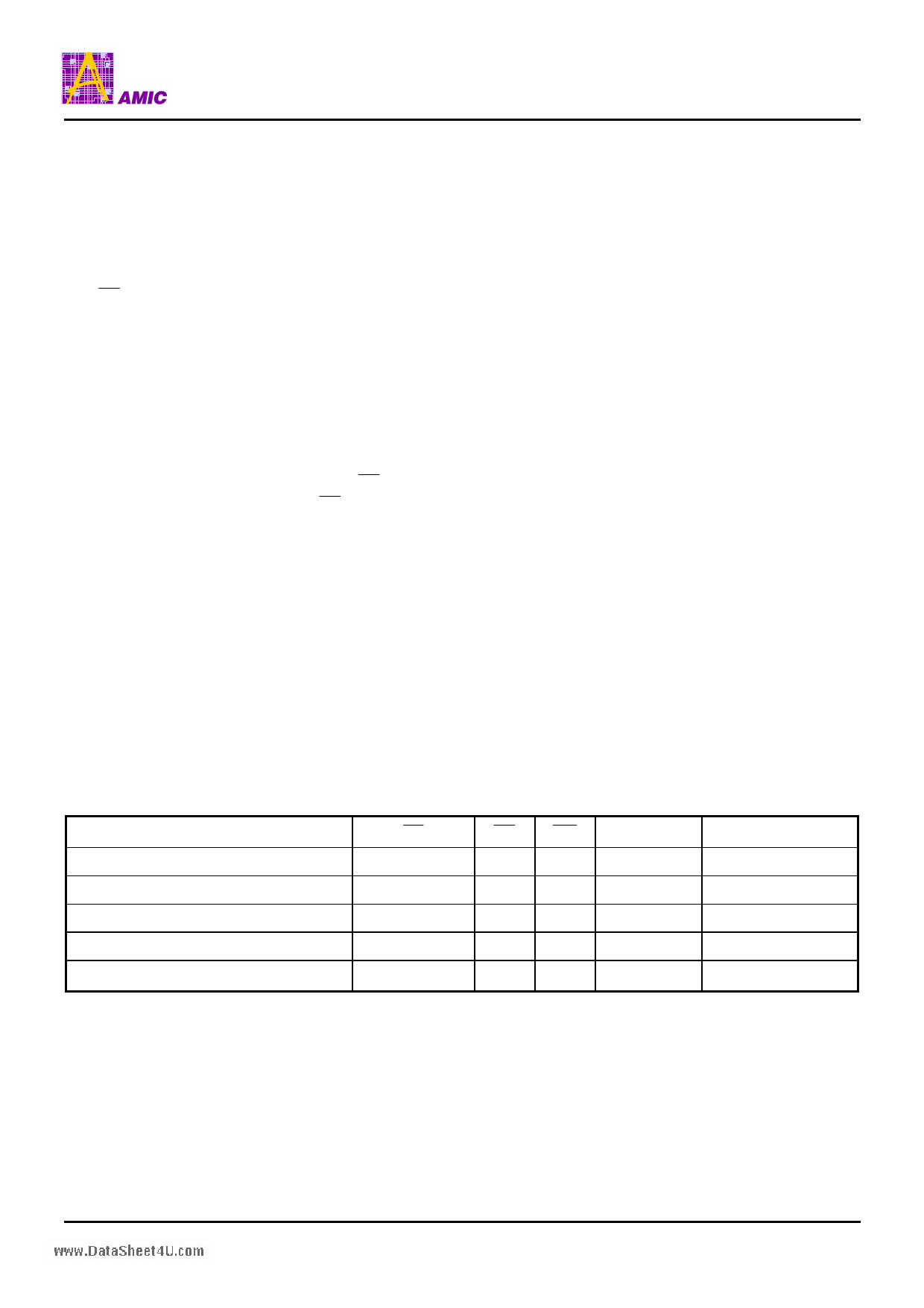
Operation
Read
Write
CMOS Standby
TTL Standby
Output Disable
Table 1. A29L040A Device Bus Operations
CE OE WE
L LH
L HL
VCC ± 0.3 V
X
X
H XX
L HH
A0 – A18
AIN
AIN
X
X
X
I/O0 - I/O7
DOUT
DIN
High-Z
High-Z
High-Z
Legend:
L = Logic Low = VIL, H = Logic High = VIH, VID = 12.0 ± 0.5V, X = Don't Care, DIN = Data In, DOUT = Data Out, AIN = Address In
Note: See the "Sector Protection/Unprotection" section, for more information.
PRELIMINARY (March, 2005, Version 0.0)
4
AMIC Technology, Corp.
5 Page 
www.DataSheet4U.com
A29L040A Series
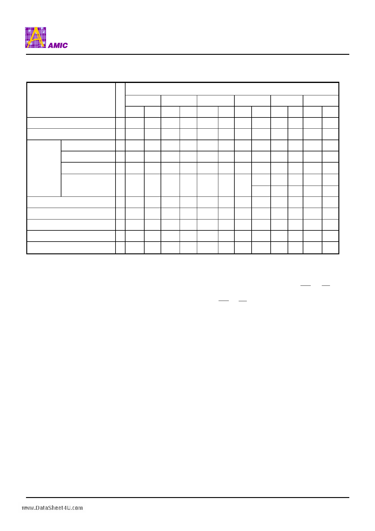
Table 4. A29L040A Command Definitions
Command
Sequence
(Note 1)
First
Second
Addr Data Addr Data
Read (Note 5)
1 RA RD
Reset (Note 6)
1 XXX F0
Manufacturer ID
4 555 AA 2AA 55
Device ID
Autoselect
(Note 7) Continuation ID
4 555 AA
4 555 AA
Sector Protect Verify 4 555 AA
(Note 8)
2AA 55
2AA 55
2AA 55
Program
Chip Erase
Sector Erase
Erase Suspend (Note 9)
Erase Resume (Note 10)
4 555 AA
6 555 AA
6 555 AA
1 XXX B0
1 XXX 30
2AA 55
2AA 55
2AA 55
Bus Cycles (Notes 2 - 4)
Third
Fourth
Fifth
Sixth
Addr Data Addr Data Addr Data Addr Data
555 90 X00 37
555 90 X01 92
555 90 X03 7F
555 90 SA 00
X02 01
555 A0 PA PD
555 80 555 AA 2AA 55 555 10
555 80 555 AA 2AA 55 SA 30
Legend:
X = Don't care
RA = Address of the memory location to be read.
RD = Data read from location RA during read operation.
PA = Address of the memory location to be programmed. Addresses latch on the falling edge of the WE or CE pulse,
whichever happens later.
PD = Data to be programmed at location PA. Data latches on the rising edge of WE or CE pulse, whichever happens first.
SA = Address of the sector to be verified (in autoselect mode) or erased. Address bits A18 - A16 select a unique sector.
Note:
1. See Table 1 for description of bus operations.
2. All values are in hexadecimal.
3. Except when reading array or autoselect data, all bus cycles are write operation.
4. Address bits A18 - A11 are don't cares for unlock and command cycles, unless SA or PA required.
5. No unlock or command cycles required when reading array data.
6. The Reset command is required to return to reading array data when device is in the autoselect mode, or if I/O5 goes high
(while the device is providing status data).
7. The fourth cycle of the autoselect command sequence is a read cycle.
8. The data is 00h for an unprotected sector and 01h for a protected sector. See "Autoselect Command Sequence" for more
information.
9. The system may read and program in non-erasing sectors, or enter the autoselect mode, when in the Erase Suspend mode.
10. The Erase Resume command is valid only during the Erase Suspend mode.
PRELIMINARY (March, 2005, Version 0.0)
10
AMIC Technology, Corp.
11 Page | ||
| Páginas | Total 30 Páginas | |
| PDF Descargar | [ Datasheet A29L040A.PDF ] | |
Hoja de datos destacado
| Número de pieza | Descripción | Fabricantes |
| A29L040 | 512K X 8 Bit CMOS 3.0 Volt-only/ Uniform Sector Flash Memory | AMIC Technology |
| A29L040-70 | 512K X 8 Bit CMOS 3.0 Volt-only/ Uniform Sector Flash Memory | AMIC Technology |
| A29L040A | 512K X 8 Bit CMOS 3.0 Volt-only Uniform Sector Flash Memory | AMIC Technology |
| A29L040L-70 | 512K X 8 Bit CMOS 3.0 Volt-only/ Uniform Sector Flash Memory | AMIC Technology |
| Número de pieza | Descripción | Fabricantes |
| SLA6805M | High Voltage 3 phase Motor Driver IC. |
Sanken |
| SDC1742 | 12- and 14-Bit Hybrid Synchro / Resolver-to-Digital Converters. |
Analog Devices |
|
DataSheet.es es una pagina web que funciona como un repositorio de manuales o hoja de datos de muchos de los productos más populares, |
| DataSheet.es | 2020 | Privacy Policy | Contacto | Buscar |
