|
|
|
PDF M28W320FSB Data sheet ( Hoja de datos )
| Número de pieza | M28W320FSB | |
| Descripción | 32Mbit (2Mb x16) and 64Mbit (4Mb x16) 3V Supply - Boot Block - Secure Flash Memories | |
| Fabricantes | STMicroelectronics | |
| Logotipo | ||
Hay una vista previa y un enlace de descarga de M28W320FSB (archivo pdf) en la parte inferior de esta página. Total 30 Páginas | ||
|
No Preview Available !
www.DataSheet4U.com
M28W320FST, M28W320FSB,
M28W640FSB, M28W640FST
32Mbit (2Mb x16) and 64Mbit (4Mb x16)
3V Supply, Boot Block, Secure Flash Memories
FEATURES SUMMARY
■ SUPPLY VOLTAGE
– VDD = 2.7V to 3.6V Core Power Supply
– VDDQ= 1.65V to 3.6V for Input/Output
– VPP = 12V for fast Program (optional)
■ ACCESS TIME: 70ns
■ PROGRAMMING TIME:
– 10µs typical
– Double Word Programming Option
– Quadruple Word Programming Option
■ COMMON FLASH INTERFACE
■ MEMORY BLOCKS
– Parameter Blocks (Top or Bottom
location)
– Main Blocks
■ HARDWARE PROTECTION
– VPP Pin for write protect of all blocks
■ SECURITY FEATURES
– 128 bit User-programmable OTP segment
– 64 bit Unique Device Identifier
– KRYPTO Features:
Modify Protection,
Read Protection,
Device Authentication
■ AUTOMATIC STAND-BY MODE
■ PROGRAM and ERASE SUSPEND
■ 100,000 PROGRAM/ERASE CYCLES per
BLOCK
■ ELECTRONIC SIGNATURE
– Manufacturer Code: 20h
– Device Codes:
M28W320FST: 880Ah,
M28W320FSB: 880Bh
M28W640FST: 8858h,
M28W640FSB: 8859h
■ ECOPACK® PACKAGE AVAILABLE
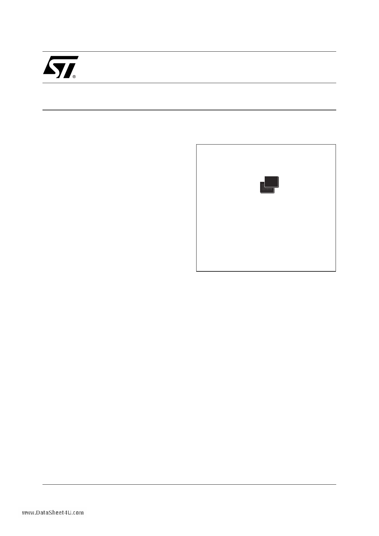
Figure 1. Package
BGA
TBGA64 (ZA)
10 x 13mm
August 2005
1/55
1 page 
www.DataSheet4U.com
M28W320FST, M28W320FSB, M28W640FST, M28W640FSB
SUMMARY DESCRIPTION
The M28W320FS and M28W640FS are 32 Mbit
(2Mbit x 16) and 64 Mbit (4Mbit x 16) Secure Flash
memories. The devices can be erased electrically
at block level and programmed in-system on a
Word-by-Word basis using a 2.7V to 3.6V VDD
supply for the circuitry and a 1.65V to 3.6V VDDQ
supply for the Input/Output pins. An optional 12V
VPP power supply is provided to speed up custom-
er programming.
The M28W320FS and M28W640FS feature
32Mbit and 64 Mbits respectively and have an
asymmetrical block architecture with 4 KWord Pa-
rameter Blocks and 32 KWord Main Blocks. The
M28W320FST and M28W640FST have the Pa-
rameter Blocks at the top of the memory address
space while the M28W320FSB and
M28W640FSB locate the Parameter Blocks start-
ing from the bottom. Refer to Table 1., Figure 5.
and Figure 6. for a detailed description of the de-
vices memory architecture and map.
All devices are equipped with hardware and soft-
ware block protection features to avoid unwanted
program/erase (modify) or read of the Flash mem-
ory content:
■ Hardware Protection:
– When VPP ≤VPPLK all blocks are protected
against program or erase.
■ Software Protection thanks to KRYPTO
Security Features:
– Modify Protection: volatile and non-
volatile.
– Read Protection.
The KRYPTO Security features are described in a
dedicated Application Note. Please contact STMi-
croelectronics for further details.
Two registers are available for protection purpose:
■ The Protection Register
■ The KRYPTO Protection Register.
The Protection Register is a 192 bit Protection
Register to increase the protection of a system de-
sign. The Protection Register is divided into a 64
bit segment and a 128 bit segment. The 64 bit seg-
ment contains a unique device number written by
ST, while the second one is one-time-programma-
ble by the user. The user programmable segment
can be permanently protected. Figure 7., shows
the Protection Register Memory Map.
The KRYPTO Protection Register is used to man-
age the Modify and Read protection modes. It also
features a Device Authentication mechanism. The
KRYPTO Protection Register is described in a
dedicated Application Note. Please contact STMi-
croelectronics for further details.
Each block can be erased separately. Erase can
be suspended in order to perform either read or
program in any other block and then resumed.
Program can be suspended to read data in any
other block and then resumed. Each block can be
programmed and erased over 100,000 cycles.
Program and Erase commands are written to the
Command Interface of the memory. An on-chip
Program/Erase Controller takes care of the tim-
ings necessary for program and erase operations.
The end of a program or erase operation can be
detected and any error conditions identified. The
command set required to control the memory is
consistent with JEDEC standards.
All the devices are offered in a TBGA64 (10 x
13mm) package.
In order to meet environmental requirements, ST
offers the M28W320FS and M28W640FS in ECO-
PACK® packages. ECOPACK packages are
Lead-free. The category of second Level Intercon-
nect is marked on the package and on the inner
box label, in compliance with JEDEC Standard
JESD97. The maximum ratings related to solder-
ing conditions are also marked on the inner box la-
bel.
ECOPACK is an ST trademark. ECOPACK speci-
fications are available at: www.st.com.
All devices are supplied with all the bits erased
(set to ’1’).
Table 1. M28W320FS and M28W640FS Memory Architecture
Device
Parameter Blocks
No. of Blocks
Block Size(1)
M28W320FS
M28W640FS
Note: 1. Erasable Block size.
8
8
4 KWords
4 KWords
No. of
Blocks
63
127
Main Blocks
Block Size
32 KWords
32 KWords
5/55
5 Page 
www.DataSheet4U.com
M28W320FST, M28W320FSB, M28W640FST, M28W640FSB
BUS OPERATIONS
There are six standard bus operations that control
the device. These are Bus Read, Bus Write, Out-
put Disable, Standby, Automatic Standby and Re-
set. See Table 3., Bus Operations, for a summary.
Typically glitches of less than 5ns on Chip Enable
or Write Enable are ignored by the memory and do
not affect bus operations.
Read. Read Bus operations are used to output
the contents of the Memory Array, the Electronic
Signature, the Status Register and the Common
Flash Interface. Both Chip Enable and Output En-
able must be at VIL in order to perform a read op-
eration. The Chip Enable input should be used to
enable the device. Output Enable should be used
to gate data onto the output. The data read de-
pends on the previous command written to the
memory (see Command Interface section). See
Figure 10., Read AC Waveforms, and Table
14., Read AC Characteristics, for details of when
the output becomes valid.
Read mode is the default state of the device when
exiting Reset or after power-up.
Write. Bus Write operations write Commands to
the memory or latch Input Data to be programmed.
A write operation is initiated when Chip Enable
and Write Enable are at VIL with Output Enable at
VIH. Commands, Input Data and Addresses are
latched on the rising edge of Write Enable or Chip
Enable, whichever occurs first.
See Figure 11. and Figure 12., Write AC Wave-
forms, and Table 15. and Table 16., Write AC
Characteristics, for details of the timing require-
ments.
Output Disable. The data outputs are high im-
pedance when the Output Enable is at VIH.
Standby. Standby disables most of the internal
circuitry allowing a substantial reduction of the cur-
rent consumption. The memory is in stand-by
when Chip Enable is at VIH and the device is in
read mode. The power consumption is reduced to
the stand-by level and the outputs are set to high
impedance, independently from the Output Enable
or Write Enable inputs. If Chip Enable switches to
VIH during a program or erase operation, the de-
vice enters Standby mode when finished.
Automatic Standby. Automatic Standby pro-
vides a low power consumption state during Read
mode. Following a read operation, the device en-
ters Automatic Standby after 150ns of bus inactiv-
ity even if Chip Enable is Low, VIL, and the supply
current is reduced to IDD1. The data Inputs/Out-
puts will still output data if a bus Read operation is
in progress.
Reset. During Reset mode when Output Enable
is Low, VIL, the memory is deselected and the out-
puts are high impedance. The memory is in Reset
mode when Reset is at VIL. The power consump-
tion is reduced to the Standby level, independently
from the Chip Enable, Output Enable or Write En-
able inputs. If Reset is pulled to VSS during a Pro-
gram or Erase, this operation is aborted and the
memory content is no longer valid.
Table 3. Bus Operations
Operation E G W RP
VPP DQ0-DQ15
Bus Read
VIL
VIL
VIH
VIH
Don't Care
Data Output
Bus Write
VIL VIH VIL VIH VDD or VPPH Data Input
Output Disable
VIL VIH VIH VIH Don't Care
Hi-Z
Standby
VIH X
X VIH Don't Care
Hi-Z
Reset
X
Note: X = VIL or VIH, VPPH = 12V ± 5%.
X
X VIL Don't Care
Hi-Z
11/55
11 Page | ||
| Páginas | Total 30 Páginas | |
| PDF Descargar | [ Datasheet M28W320FSB.PDF ] | |
Hoja de datos destacado
| Número de pieza | Descripción | Fabricantes |
| M28W320FSB | 32Mbit (2Mb x16) and 64Mbit (4Mb x16) 3V Supply - Boot Block - Secure Flash Memories | STMicroelectronics |
| M28W320FST | 32Mbit (2Mb x16) and 64Mbit (4Mb x16) 3V Supply - Boot Block - Secure Flash Memories | STMicroelectronics |
| Número de pieza | Descripción | Fabricantes |
| SLA6805M | High Voltage 3 phase Motor Driver IC. |
Sanken |
| SDC1742 | 12- and 14-Bit Hybrid Synchro / Resolver-to-Digital Converters. |
Analog Devices |
|
DataSheet.es es una pagina web que funciona como un repositorio de manuales o hoja de datos de muchos de los productos más populares, |
| DataSheet.es | 2020 | Privacy Policy | Contacto | Buscar |