|
|
PDF VN5050J-E Data sheet ( Hoja de datos )
| Número de pieza | VN5050J-E | |
| Descripción | Single channel high side driver | |
| Fabricantes | STMicroelectronics | |
| Logotipo |  |
|
Hay una vista previa y un enlace de descarga de VN5050J-E (archivo pdf) en la parte inferior de esta página. Total 30 Páginas | ||
|
No Preview Available !
www.DataSheet4U.com
VN5050J-E
Single channel high side driver
for automotive applications
Features
Max supply voltage
Operating voltage range
Max On-State resistance (per ch.)
Current limitation (typ)
Off state supply current
VCC
VCC
RON
ILIMH
IS
(1) Typical value with all loads connected
41V
4.5 to 36V
50 mΩ
19 A
2 µA(1)
PowerSSO-12
Application
■ Main
– Inrush current active management by
power limitation
– Very low stand-by current
– 3.0V CMOS compatible input
– Optimized electromagnetic emission
– Very low electromagnetic susceptibility
– In compliance with the 2002/95/EC
European directive
■ Diagnostic functions
– Open drain status output
– On state open load detection
– Off state open load detection
– Thermal shutdown indication
■ Protections
– Undervoltage shut-down
– Overvoltage clamp
– Output stuck to VCC detection
– Load current limitation
– Self limiting of fast thermal transients
– Protection against loss of ground and loss
of VCC
– Thermal shut down
– Reverse battery protection (see Figure 27)
– Electrostatic discharge protection
Table 1. Device summary
■ All types of resistive, inductive and capacitive
loads
Description
The VN5050J-E is a monolithic device made
using STMicroelectronics VIPower technology. It
is intended for driving resistive or inductive loads
with one side connected to ground. Active VCC pin
voltage clamp protects the device against low
energy spikes (see ISO7637 transient
compatibility table). The device detects open load
condition both in on and off state, when STAT_DIS
is left open or driven low. Output shorted to VCC is
detected in the off state.
When STAT_DIS is driven high, the STATUS pin
is in a high impedance condition.Output current
limitation protects the device in overload
condition. In case of long duration overload, the
device limits the dissipated power to safe level up
to thermal shut-down intervention.Thermal shut-
down with automatic restart allows the device to
recover normal operation as soon as fault
condition disappears.
Package
Tube
Order codes
Tape & Reel
PowerSSO-12
VN5050J-E
VN5050JTR-E
September 2007
Rev 2
1/31
www.st.com
31
1 page 
VN5050J-E
Block diagram anwdwpwi.nDadteasShceriept4tiUo.cnom
1 Block diagram and pin description
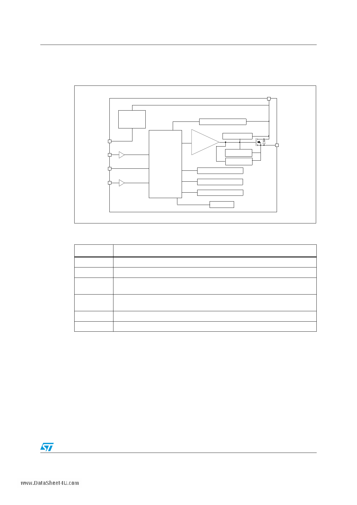
Figure 1. Block diagram
VCC
GND
INPUT
STATUS
STAT_DIS
VCC
CLAMP
LOGIC
UNDERVOLTAGE
DRIVER
PwCLAMP
ILIM
VDSLIM
OPENLOAD ON
OPENLOAD OFF
OVERTEMP.
PwrLIM
OUTPUT
Table 2. Pin function
Name
Function
VCC
OUTPUT
GND
INPUT
Battery connection
Power output
Ground connection. Must be reverse battery protected by an external diode/resistor
network
Voltage controlled input pin with hysteresis, CMOS compatible. Controls output
switch state
STATUS
STAT_DIS
Open drain digital diagnostic pin
Active high CMOS compatible pin, to disable the STATUS pin
5/31
5 Page 
VN5050J-E
Electricwawlws.pDeactaifSihceaetti4oUn.csom
Table 10. Openload detection
Symbol
Parameter
Test conditions
Openload ON State
IOL Detection Threshold
VIN = 5V ,8V<VCC<18V
tDOL(on)
tPOL
VOL
tDSTKON
Openload ON State
Detection Delay
IOUT = 0A, VCC=13V
(see Figure 4)
Delay between INPUT
falling edge and STATUS
rising edge in Openload
condition
IOUT = 0A (see Figure 4)
Openload OFF State
Voltage Detection
Threshold
VIN = 0V, 8V<VCC<16V
Output Short Circuit to
VCC Detection Delay at
Turn Off
(see Figure 4)
Min Typ Max Unit
10
See
Figure 18
50
mA
200 µs
200 500 1000 µs
2
See
Figure 19
4
V
180 tPOL µs
Table 11. Logic input
Symbol
Parameter
Test conditions
VIL
IIL
VIH
IIH
VI(hyst)
VICL
VSDL
Input Low Level
Low Level Input Current VIN =0.9 V
Input High Level
High Level Input Current VIN = 2.1 V
Input Hysteresis Voltage
Input Clamp Voltage
STAT_DIS low level
voltage
IIN = 1mA
IIN = -1mA
ISDL
Low level STAT_DIS
current
VSD = 0.9 V
VSDH
STAT_DIS high level
voltage
ISDH
High level STAT_DIS
current
VSD = 2.1 V
VSD(hyst)
STAT_DIS hysteresis
voltage
VSDCL
STAT_DIS clamp voltage ISD=1mA
ISD=-1mA
Min. Typ. Max. Unit
1
2.1
0.25
5.5
-0.7
0.9
10
7
V
µA
V
µA
V
V
V
0.9 V
1 µA
2.1 V
10 µA
0.25
5.5
-0.7
7
V
V
V
11/31
11 Page | ||
| Páginas | Total 30 Páginas | |
| PDF Descargar | [ Datasheet VN5050J-E.PDF ] | |
Hoja de datos destacado
| Número de pieza | Descripción | Fabricantes |
| VN5050J-E | Single channel high side driver | STMicroelectronics |
| Número de pieza | Descripción | Fabricantes |
| SLA6805M | High Voltage 3 phase Motor Driver IC. |
Sanken |
| SDC1742 | 12- and 14-Bit Hybrid Synchro / Resolver-to-Digital Converters. |
Analog Devices |
|
DataSheet.es es una pagina web que funciona como un repositorio de manuales o hoja de datos de muchos de los productos más populares, |
| DataSheet.es | 2020 | Privacy Policy | Contacto | Buscar |
