|
|
|
PDF VN920SO-E Data sheet ( Hoja de datos )
| Número de pieza | VN920SO-E | |
| Descripción | HIGH SIDE DRIVER | |
| Fabricantes | STMicroelectronics | |
| Logotipo | ||
Hay una vista previa y un enlace de descarga de VN920SO-E (archivo pdf) en la parte inferior de esta página. Total 24 Páginas | ||
|
No Preview Available !
www.DataSheet4U.com
VN920-E
VN920B5-E / VN920SO-E
HIGH SIDE DRIVER
Table 1. General Features
Type
RDS(on)
VN920-E
VN920B5-E
VN920SO-E
16mΩ
IOUT
30 A
VCC
36 V
s CMOS COMPATIBLE INPUT
s PROPORTIONAL LOAD CURRENT SENSE
s SHORTED LOAD PROTECTION
s UNDERVOLTAGE AND OVERVOLTAGE
SHUTDOWN
s OVERVOLTAGE CLAMP
s THERMAL SHUTDOWN
s CURRENT LIMITATION
s PROTECTION AGAINST LOSS OF GROUND
AND LOSS OF VCC
s VERY LOW STAND-BY POWER DISSIPATION
s REVERSE BATTERY PROTECTION (*)
s IN COMPLIANCE WITH THE 2002/95/EC
EUROPEAN DIRECTIVE
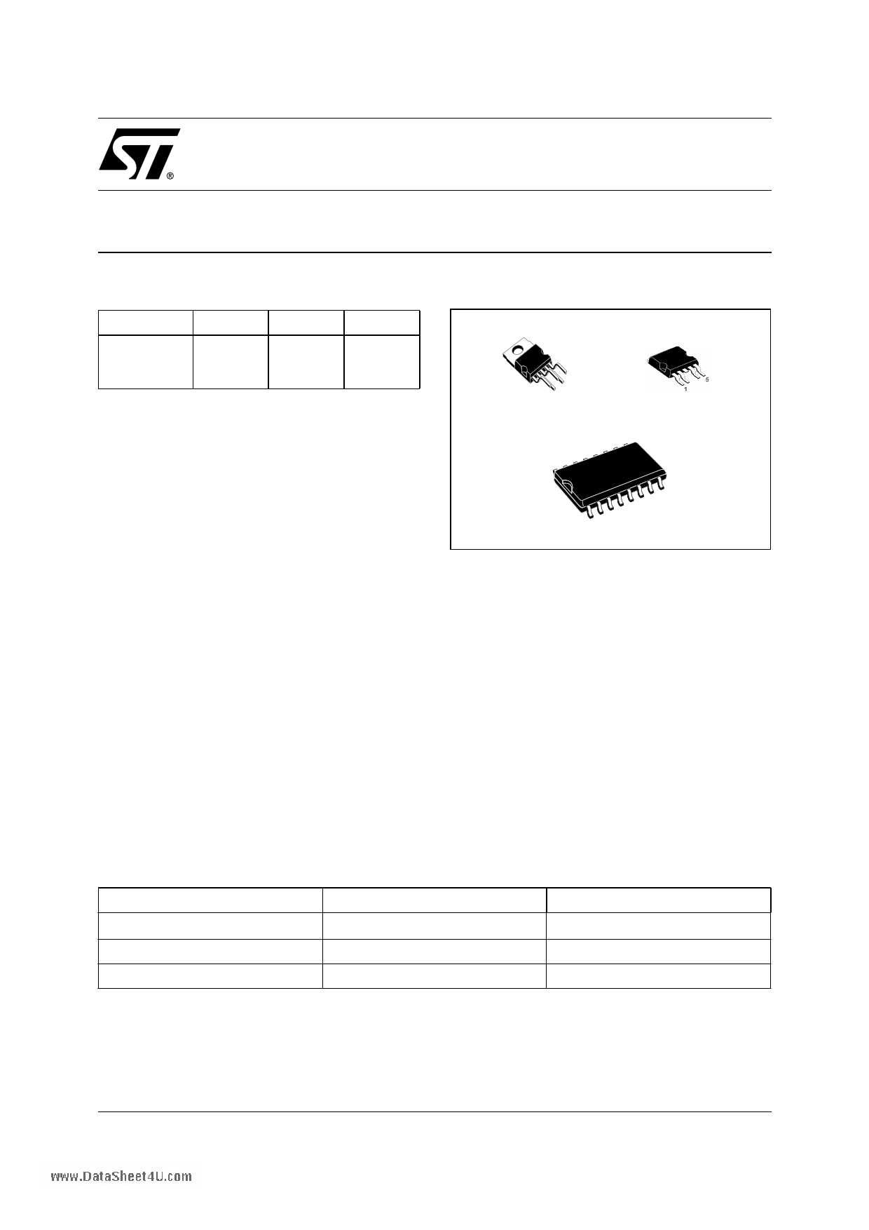
Figure 1. Package
PENTAWATT
P2PAK
SO-16L
Active current limitation combined with thermal
shutdown and automatic restart protect the device
against overload. The device integrates an analog
current sense output which delivers a current
proportional to the load current. Device
automatically turns off in case of ground pin
disconnection.
DESCRIPTION
The VN920-E, VN920B5-E, VN920SO-E is a
monolithic device made by using
STMicroelectronics VIPower M0-3 Technology,
intended for driving any kind of load with one side
connected to ground. Active VCC pin voltage
clamp protects the device against low energy
spikes (see ISO7637 transient compatibility table).
Table 2. Order Codes
Package
PENTAWATT
P2PAK
SO-16L
Tube
VN920-E
VN920B5-E
VN920SO-E
Tape and Reel
-
VN920B5TR-E
VN920SOTR-E
Note: (*) See application schematic at page 9.
October 2004
Rev. 1
1/24
1 page 
www.DataSheet4U.com
VN920-E / VN920B5-E / VN920SO-E
ELECTRICAL CHARACTERISTICS (continued)
Table 8. VCC - Output Diode
Symbol
Parameter
VF Forward on Voltage
Test Conditions
-IOUT=2A; Tj=150°C
Min.
Typ.
Max.
0.6
Unit
V
Table 9. Protections (see note 1)
Symbol
TTSD
TR
Thyst
Parameter
Shut-down Temperature
Reset Temperature
Thermal Hysteresis
Ilim DC Short Circuit Current
Vdemag
VON
Turn-off Output Clamp
Voltage
Output Voltage Drop
Limitation
Test Conditions
VCC=13V
5V<VCC<36V
IOUT=2A; VIN=0V; L=6mH
IOUT=1A; Tj=-40°C....+150°C
Min Typ Max Unit
150 175 200 °C
135 °C
7 15
°C
30 45 75 A
75 A
VCC-41 VCC-48 VCC-55 V
50 mV
Note: 1. To ensure long term reliability under heavy overload or short circuit conditions, protection and related diagnostic signals must be
used together with a proper software strategy. If the device is subjected to abnormal conditions, this software must limit the duration
and number of activation cycles.
Table 10. Current Sense (9V≤VCC≤16V) (See Fig. 5)
Symbol
K1
dK1/K1
K2
dK2/K2
K3
dK3/K3
Parameter
IOUT/ISENSE
Current Sense Ratio Drift
IOUT/ISENSE
Current Sense Ratio Drift
IOUT/ISENSE
Current Sense Ratio Drift
Test Conditions
IOUT=1A; VSENSE=0.5V;
Tj= -40°C...150°C
IOUT=1A; VSENSE=0.5V;
Tj= -40°C...+150°C
IOUT=10A; VSENSE=4V; Tj=-40°C
Tj=25°C...150°C
IOUT=10A; VSENSE=4V;
Tj=-40°C...+150°C
IOUT=30A; VSENSE=4V; Tj=-40°C
Tj=25°C...150°C
IOUT=30A; VSENSE=4V;
Tj=-40°C...+150°C
Min
3300
Typ
4400
Max
6000
Unit
-10
4200
4400
-8
4200
4400
-6
4900
4900
4900
4900
+10
6000
5750
+8
5500
5250
+6
%
%
%
ISENSEO
Analog Sense Leakage
Current
VCC=6...16V; IOUT=0A;VSENSE=0V;
Tj=-40°C...+150°C
0
10 µA
VSENSE
VSENSEH
RVSENSEH
tDSENSE
Max Analog Sense Output
Voltage
Sense Voltage in
Overtemperature
conditions
Analog Sense Output
Impedance in
Overtemperature
Condition
Current sense delay
response
VCC=5.5V; IOUT=5A; RSENSE=10KΩ
VCC>8V; IOUT=10A; RSENSE=10KΩ
VCC=13V; RSENSE=3.9KΩ
VCC=13V; Tj>TTSD; Output Open
to 90% ISENSE (see note 2)
2
4
5.5
V
V
V
400 Ω
500 µs
Note: 2. current sense signal delay after positive input slope.
5/24
5 Page 
Figure 15. Input Low Level
Vil (V)
2.6
2.4
2.2
2
1.8
1.6
1.4
1.2
1
-50 -25 0 25 50 75 100 125 150 175
Tc (°C)
Figure 16. Turn-on Voltage Slope
dVout/dt(on) (V/ms)
700
650
Vcc=13V
600
Rl=1.3Ohm
550
500
450
400
350
300
250
-50 -25 0 25 50 75 100 125 150 175
Tc (ºC)
Figure 17. Overvoltage Shutdown
Vov (V)
50
48
46
44
42
40
38
36
34
32
30
-50
-25
0
25 50 75 100 125 150 175
Tc (°C)
www.DataSheet4U.com
VN920-E / VN920B5-E / VN920SO-E
Figure 18. Input Hysteresis Voltage
Vhyst (V)
1.5
1.4
1.3
1.2
1.1
1
0.9
0.8
0.7
0.6
0.5
-50 -25 0 25 50 75 100 125 150 175
Tc (°C)
Figure 19. Turn-off Voltage Slope
dVout/dt(off) (V/ms)
550
500
450 Vcc=13V
Rl=1.3Ohm
400
350
300
250
200
150
100
50
0
-50 -25 0 25
50 75
Tc (°C)
100 125 150 175
Figure 20. ILIM Vs Tcase
Ilim (A)
100
90
Vcc=13V
80
70
60
50
40
30
20
10
0
-50 -25 0 25 50 75 100 125 150 175
Tc (°C)
11/24
11 Page | ||
| Páginas | Total 24 Páginas | |
| PDF Descargar | [ Datasheet VN920SO-E.PDF ] | |
Hoja de datos destacado
| Número de pieza | Descripción | Fabricantes |
| VN920SO-E | HIGH SIDE DRIVER | STMicroelectronics |
| Número de pieza | Descripción | Fabricantes |
| SLA6805M | High Voltage 3 phase Motor Driver IC. |
Sanken |
| SDC1742 | 12- and 14-Bit Hybrid Synchro / Resolver-to-Digital Converters. |
Analog Devices |
|
DataSheet.es es una pagina web que funciona como un repositorio de manuales o hoja de datos de muchos de los productos más populares, |
| DataSheet.es | 2020 | Privacy Policy | Contacto | Buscar |