|
|
|
PDF LC78835K Data sheet ( Hoja de datos )
| Número de pieza | LC78835K | |
| Descripción | 18 Bits Digital Filter and D/A Converter for Digital Audio | |
| Fabricantes | Sanyo Semicon Device | |
| Logotipo | ||
Hay una vista previa y un enlace de descarga de LC78835K (archivo pdf) en la parte inferior de esta página. Total 14 Páginas | ||
|
No Preview Available !
Ordering number : EN4624B
CMOS IC
LC78835K, 78835KM
18 Bits Digital Filter and D/A Converter
for Digital Audio
Overview
The LC78835K and 78835KM are 18-bit digital-to-analog
D/A converter CMOS ICs with an on-chip eight-times
oversampling digital filter. The LC78835 and the
LC78835M are pin compatible.
Features
• Digital filter
— 8 fs oversampling filter: 3-stage finite-impulse-
response (FIR) filter design (43rd-, 11th-, and third-
orders)
— De-emphasis filter: Supports fs = 32 kHz, 44.1 kHz,
or 48 kHz
— Soft mute
— Noise shaper
— Supports double-rate sampling
• D/A converter
— Dynamic level-shifting 18-bit digital-to-analog
converter
— On-chip 2-channel D/A converter (with
corresponding output)
— On-chip output op-amp
— Supports 384 fs, 392 fs, 448 fs, or 512 fs system
clock
— Single 5 V supply
— Permits low-voltage operation (3.5 V)
— Low-power silicon-gate CMOS process
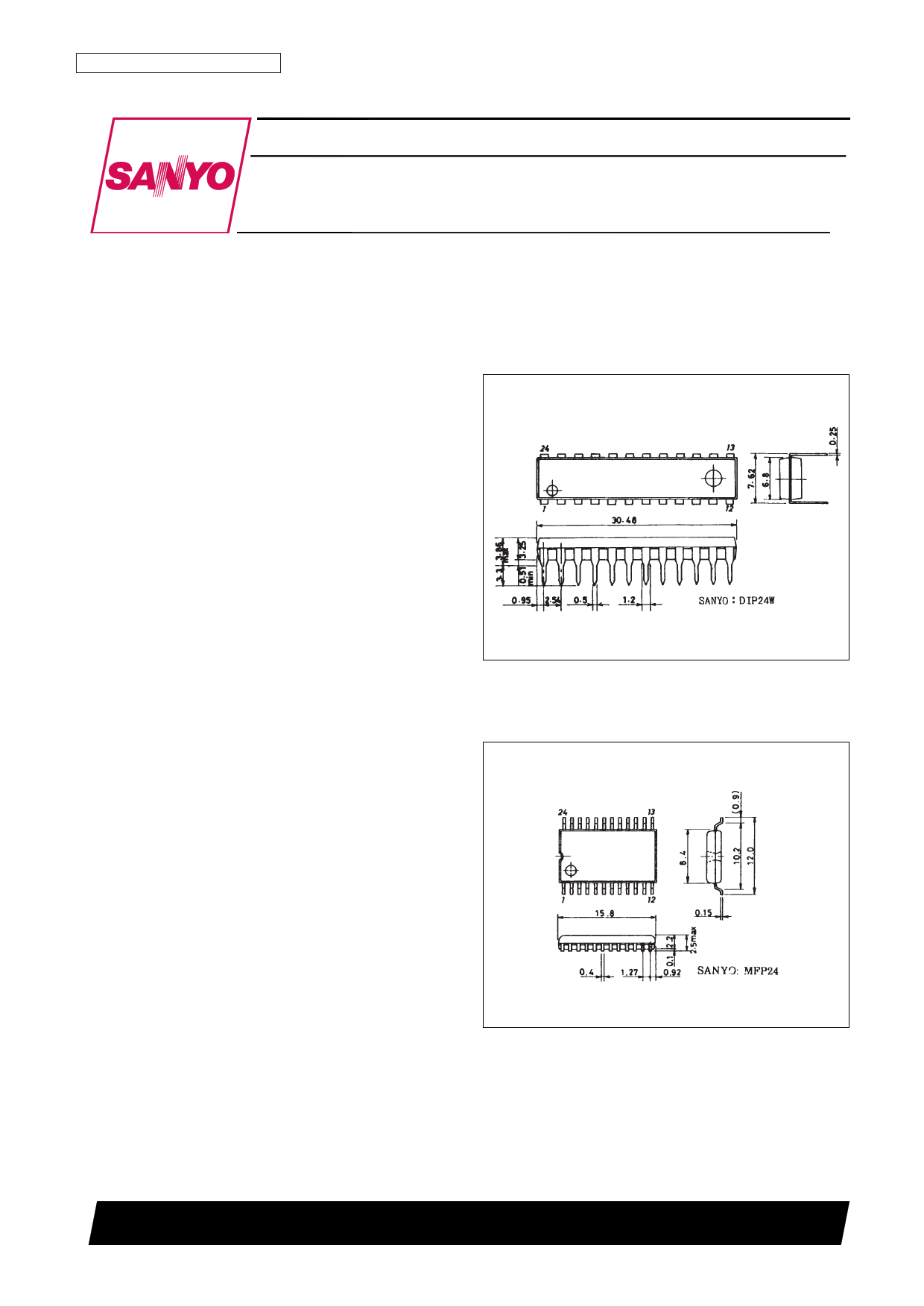
Package Dimensions
unit: mm
3092-DIP24W
[LC78835K]
unit: mm
3155-MFP24
[LC78835KM]
SANYO: DIP24W
SANYO: MFP24
SANYO Electric Co.,Ltd. Semiconductor Bussiness Headquarters
TOKYO OFFICE Tokyo Bldg., 1-10, 1 Chome, Ueno, Taito-ku, TOKYO, 110 JAPAN
73696HA (OT)/N1094TH (OT)/82793JN No. 4624-1/14
1 page 
Pin Description
Number
1
2
3
4
5
6
7
8
9
Name
REFH
VrefH
MUTE
D/N
BCLK
DATA
LRCK
DVDD
CKOUT
10 XOUT
11 XIN
12 DGND
13 INITB
14 EMP
15 FS1
16 FS2
LC78835K, 78835KM
Description
Reference voltage “H” pin
Normally connected to AGND via a capacitor
Reference voltage “H” input pin
Mute signal input pin
Soft mute is on when high
Normal/double-speed operation toggle
Double-speed operation when high, normal operation when low
Bit clock input pin
Digital audio data input pin
2’s complement code, with input from the most significant bit (MSB)
Left-right clock input pin
Channel 1 when high, channel 2 when low
Digital power supply pin
Clock output pin
When at 392 fs: 196 fs clock
When not at 392 fs: XIN-frequency clock
Crystal oscillator output pin (system clock output pin)
Crystal oscillator input pin (system clock input pin)
Digital ground pin
Initialization signal input pin
Initialization performed when low
On/Off toggle for the de-emphasis filter
On when high, off when low
32 kHz/44.1 kHz/48 kHz selector for the de-emphasis filter
FS1 L H H L
FS2 L L H H
fs
44.1 kHz
32 kHz 48 kHz
17
CKSL1
System clock selector pin
CKSL1 CKSL2 System Clock
LL
384 fs
18 CKSL2
LH
HL
392 fs
448 fs
HH
512 fs
19
VrefL
Reference voltage “L” input pin
20
REFL
Reference voltage “L” pin
Normally connected to AGND via a capacitor
21
CH2OUT
Channel 2 analog output pin
22
AGND
Analog ground pin
23
CH1OUT
Channel 1 analog output pin
24
AVDD
Analog power supply pin
No. 4624-5/14
5 Page 
LC78835K, 78835KM
• Pulse-Width Modulation (PWM) D/A Converter
This is a 3-bit circuit that applies pulse width modulation to voltages V2 and V1 output from the R-string D/A
converter to produce an 8-way division. Depending on the value of the data in bits D8 to D6, one of the voltages,
V2 or V1, is output to the CH1OUT (or CH2OUT) pin.
• Level Shift D/A Converter
The variable resistors VRH and VRL are connected in series to the two ends of the R-string D/A converter
resistance, configuring a 6-bit D/A conversion circuit. Depending on the values of the data in the LSBs (bits D5 to
D0), VRH and VRL change as follows.
(1) The sum of VRH and VRL is constant, irrespective of the data value.
(2) Irrespective of the data value, VRH and VRL are in the range of 0 to 63R/512 (where R is the unit resistance of
the R-string D/A converter) and resistance changes in R/512 steps in accordance with the data value.
This means that the R-string D/A converter outputs, V2 and V1, each vary in the range of 0 to 63 × ∆V/512 (∆V =
(VH - VL)/512) in ∆V/512 steps.
— Vref H/L, REF H/L Pins
The voltage on the Vref pins, used to apply the reference voltage to the resistance strings, are usually set so that
VrefH = AVDD and VrefL = AGND. In addition, a 10 µF rated condenser connects REFH and AGND as well
as REFL and AGND. When VrefH = 5.0 V, VrefL = 0 V, the LC78835K on-chip RH and RL resistors
maximum output amplitude at 0 dB playback is output in the 3.0 Vp-p range extending from a minimum 0.6 V
to maximum 3.6 V.
No. 4624-11/14
11 Page | ||
| Páginas | Total 14 Páginas | |
| PDF Descargar | [ Datasheet LC78835K.PDF ] | |
Hoja de datos destacado
| Número de pieza | Descripción | Fabricantes |
| LC78835 | 18 Bits Digital Filter and D/A Converter for Digital Audio | Sanyo Semicon Device |
| LC78835K | 18 Bits Digital Filter and D/A Converter for Digital Audio | Sanyo Semicon Device |
| LC78835KM | 18 Bits Digital Filter and D/A Converter for Digital Audio | Sanyo Semicon Device |
| Número de pieza | Descripción | Fabricantes |
| SLA6805M | High Voltage 3 phase Motor Driver IC. |
Sanken |
| SDC1742 | 12- and 14-Bit Hybrid Synchro / Resolver-to-Digital Converters. |
Analog Devices |
|
DataSheet.es es una pagina web que funciona como un repositorio de manuales o hoja de datos de muchos de los productos más populares, |
| DataSheet.es | 2020 | Privacy Policy | Contacto | Buscar |