|
|
PDF TC59LM906AMG-37 Data sheet ( Hoja de datos )
| Número de pieza | TC59LM906AMG-37 | |
| Descripción | MOS DIGITAL INTEGRATED CIRCUIT SILICON MONOLITHIC | |
| Fabricantes | Toshiba Semiconductor | |
| Logotipo | ||
Hay una vista previa y un enlace de descarga de TC59LM906AMG-37 (archivo pdf) en la parte inferior de esta página. Total 30 Páginas | ||
|
No Preview Available !
TC59LM914/06AMG-37,-50
TENTATIVE TOSHIBA MOS DIGITAL INTEGRATED CIRCUIT SILICON MONOLIwTHwwIC.DataSheet4U.com
512Mbits Network FCRAM1 (SSTL_18 / HSTL_Interface)
− 4,194,304-WORDS × 8 BANKS × 16-BITS
− 8,388,608-WORDS × 8 BANKS × 8-BITS
DESCRIPTION
Network FCRAMTM is Double Data Rate Fast Cycle Random Access Memory. TC59LM914/06AMG is Fast Cycle
Random Access Memory (Network FCRAMTM) containing 536,870,912 memory cells. TC59LM914AMG is organized
as 4,194,304-words × 8 banks × 16 bits, TC59LM906AMG is organized as 8,388,608-words × 8 banks × 8 bits.
TC59LM914/06AMG feature a fully synchronous operation referenced to clock edge whereby all operations are
synchronized at a clock input which enables high performance and simple user interface coexistence.
TC59LM914/06AMG can operate fast core cycle compared with regular DDR SDRAM.
TC59LM914/06AMG is suitable for Network, Server and other applications where large memory density and low
power consumption are required. The Output Driver for Network FCRAMTM is capable of high quality fast data
transfer under light loading condition.
FEATURES
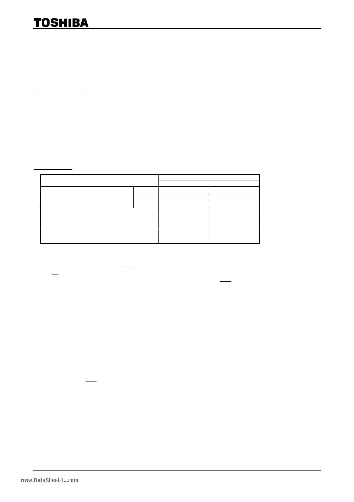
PARAMETER
TC59LM914/06
-37 -50
CL = 3
5.5 ns
6.0 ns
tCK Clock Cycle Time (min)
CL = 4
4.5 ns
5.5 ns
CL = 5
3.75 ns
5.0 ns
tRC Random Read/Write Cycle Time (min)
22.5 ns
27.5 ns
tRAC Random Access Time (max)
22.0 ns
24.0 ns
IDD1S Operating Current (single bank) (max)
280 mA
240 mA
lDD2P Power Down Current (max)
90 mA
80 mA
lDD6 Self-Refresh Current (max)
20 mA
20 mA
• Fully Synchronous Operation
• Double Data Rate (DDR)
Data input/output are synchronized with both edges of DQS.
• Differential Clock (CLK and CLK ) inputs
CS , FN and all address input signals are sampled on the positive edge of CLK.
Output data (DQs and DQS) is aligned to the crossings of CLK and CLK .
• Fast clock cycle time of 3.75 ns minimum
Clock: 266 MHz maximum
Data: 533 Mbps/pin maximum
• Fast cycle and Short Latency
• Eight independent banks operation
When BA2 input assign to A14 input, TC59LM914/06AMG can function as 4 bank device
(Keep backward compatibility to 256Mb)
• Bidirectional differential data strobe signal : TC59LM906AMG
• Bidirectional data strobe signal per byte : TC59LM914AMG
• Distributed Auto-Refresh cycle in 3.9 µs
• Self-Refresh
• Power Down Mode
• Variable Write Length Control
• Write Latency = CAS Latency-1
• Programable CAS Latency and Burst Length
CAS Latency = 3, 4, 5
Burst Length = 2, 4
• Organization: TC59LM914AMG : 4,194,304 words × 8 banks × 16 bits
TC59LM906AMG : 8,388,608 words × 8 banks × 8 bits
• Power Supply Voltage VDD: 2.5 V ± 0.125V
VDDQ: 1.4 V ∼ 1.9 V
• 1.8 V CMOS I/O comply with SSTL_18 and HSTL
• Package:
60Ball BGA, 1mm × 1mm Ball pitch (P−BGA64−1317−1.00AZ)
Notice : FCRAM is trademark of Fujitsu Limited, Japan.
Rev 1.0
2004-08-20 1/59
1 page 
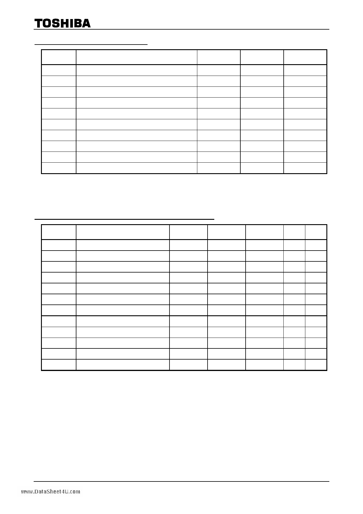
ABSOLUTE MAXIMUM RATINGS
TC59LM914/06AMG-37,-50
www.DataSheet4U.com
SYMBOL
PARAMETER
RATING
UNIT
NOTES
VDD Power Supply Voltage
−0.3~ 3.3
V
VDDQ
Power Supply Voltage (for I/O buffer)
−0.3~VDD+ 0.3
V
VIN Input Voltage
−0.3~VDD+ 0.3
V
VOUT
Output and I/O pin Voltage
−0.3~VDDQ + 0.3
V
VREF
Input Reference Voltage
−0.3~VDD+ 0.3
V
Topr Operating Temperature (case)
0~85
°C
Tstg Storage Temperature
−55~150
°C
Tsolder
Soldering Temperature (10 s)
260 °C
PD Power Dissipation
2W
IOUT
Short Circuit Output Current
±50 mA
Caution: Conditions outside the limits listed under “ABSOLUTE MAXIMUM RATINGS” may cause permanent damage to the device.
The device is not meant to be operated under conditions outside the limits described in the operational section of this
specification.
Exposure to “ABSOLUTE MAXIMUM RATINGS” conditions for extended periods may affect device reliability.
RECOMMENDED DC, AC OPERATING CONDITIONS (Notes: 1)(TCASE = 0~85°C)
SYMBOL
PARAMETER
MIN
VDD
VDDQ
VREF
VIH (DC)
VIL (DC)
VICK (DC)
VID (DC)
VIH (AC)
VIL (AC)
VID (AC)
VX (AC)
VISO (AC)
Power Supply Voltage
2.375
Power Supply Voltage (for I/O buffer)
1.4
Input Reference Voltage
Input DC High Voltage
Input DC Low Voltage
VDDQ/2 × 95%
VREF + 0.125
−0.1
Differential DC Input Voltage
−0.1
Input DC Differential Voltage.
0.4
Input AC High Voltage
Input AC Low Voltage
VREF + 0.2
−0.1
Input AC Differential Voltage
0.5
Differential AC Input Cross Point Voltage VDDQ/2 − 0.125
Differential AC Middle Level
VDDQ/2 − 0.125
TYP.
2.5
⎯
VDDQ/2
⎯
⎯
⎯
⎯
⎯
⎯
⎯
⎯
⎯
MAX
UNIT NOTES
2.625
1.9
VDDQ/2 × 105%
VDDQ + 0.2
VREF − 0.125
VDDQ + 0.1
VDDQ + 0.2
VDDQ + 0.2
VREF − 0.2
VDDQ + 0.2
VDDQ/2 + 0.125
VDDQ/2 + 0.125
V
V
V
V
V
V
V
V
V
V
V
V
2
5
5
10
7, 10
3, 6
4, 6
7, 10
8, 10
9, 10
Rev 1.0
2004-08-20 5/59
5 Page 
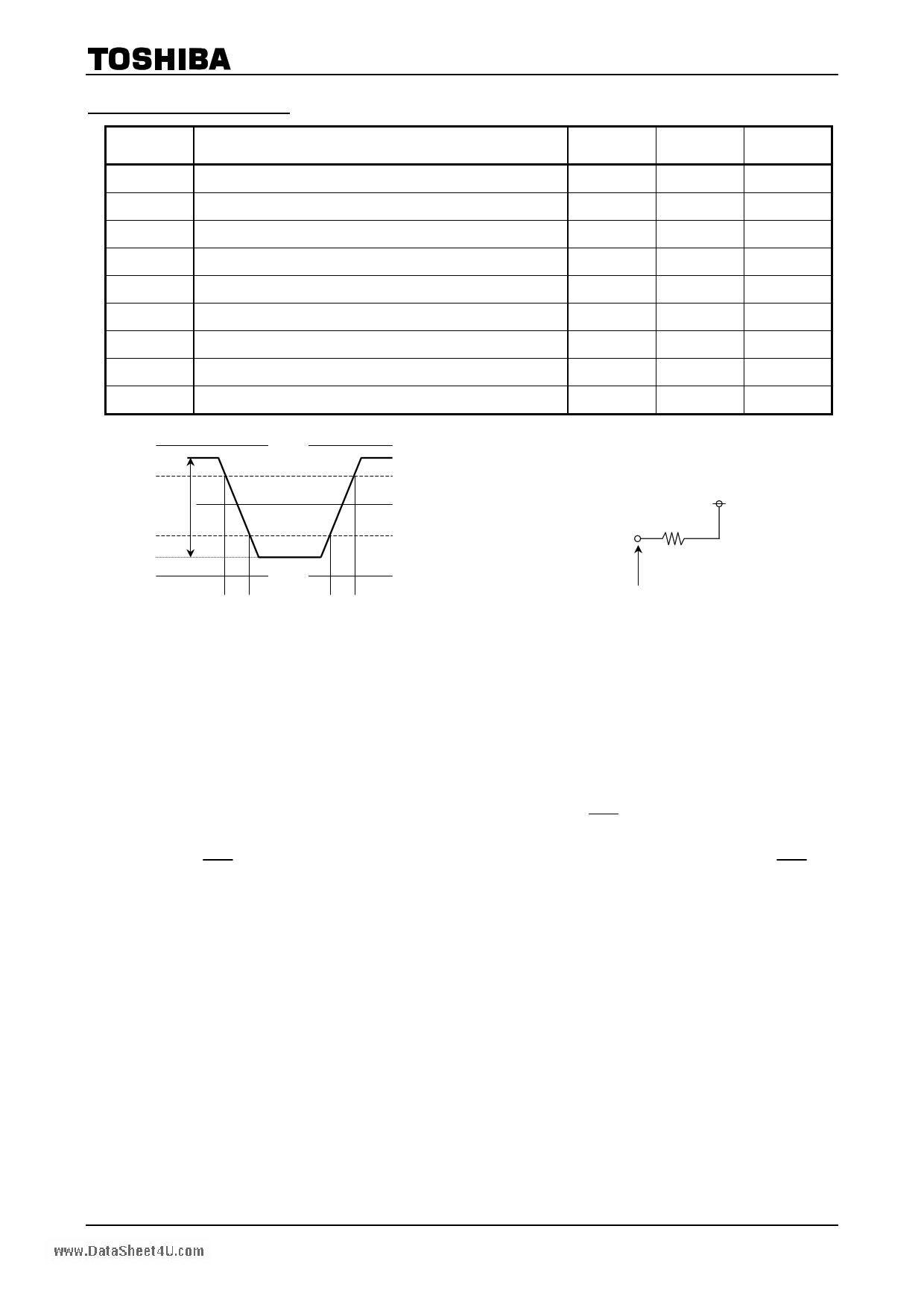
AC TEST CONDITIONS
TC59LM914/06AMG-37,-50
www.DataSheet4U.com
SYMBOL
PARAMETER
VIH (min)
VIL (max)
VREF
VTT
VSWING
Vr
VID (AC)
SLEW
VOTR
Input High Voltage (minimum)
Input Low Voltage (maximum)
Input Reference Voltage
Termination Voltage
Input Signal Peak to Peak Swing
Differential Clock Input Reference Level
Input Differential Voltage
Input Signal Minimum Slew Rate
Output Timing Measurement Reference Voltage
VALUE
VREF + 0.2
VREF − 0.2
VDDQ/2
VREF
0.7
VX (AC)
1.0
2.5
VDDQ/2
UNIT
V
V
V
V
V
V
V
V/ns
V
NOTES
9
VSWING
VDDQ
VIH min (AC)
VREF
VIL max (AC)
Output
25 Ω
VTT
Note:
VSS
∆T ∆T
SLEW = (VIH min (AC) − VIL max (AC))/∆T
Measurement point
AC Test Load
(1) Transition times are measured between VIH min (DC) and VIL max (DC).
Transition (rise and fall) of input signals have a fixed slope.
(2) If the result of nominal calculation with regard to tCK contains more than one decimal place, the result is
rounded up to the nearest decimal place.
(i.e., tDQSS = 0.75 × tCK, tCK = 5 ns, 0.75 × 5 ns = 3.75 ns is rounded up to 3.8 ns.)
(3) These parameters are measured from the differential clock (CLK and CLK ) AC cross point.
(4) These parameters are measured from signal transition point of DQS crossing VREF level.
In case of DQS enable mode, these parameters are measured from the crossing point of DQS and DQS .
(5) The tREFI (max) applies to equally distributed refresh method.
The tREFI (min) applies to both burst refresh method and distributed refresh method.
In such case, the average interval of eight consecutive Auto-Refresh commands has to be more than 400 ns
always. In other words, the number of Auto-Refresh cycles which can be performed within 3.2 µs (8 × 400 ns)
is to 8 times in the maximum.
(6) Low Impedance State is specified at VDDQ/2 ± 0.2 V from steady state.
(7) High Impedance State is specified where output buffer is no longer driven.
(8) These parameters depend on the clock jitter. These parameters are measured at stable clock.
(9) Output timing is measured by using Normal driver strength at VDDQ = 1.7V∼1.9V.
Output timing is measured by using Strong driver strength at VDDQ = 1.4V∼1.6V.
(10) These parameters are measured at tCK = minimum∼6.0ns. When tCK is longer than 6.0ns, these parameters
are specified as below for all Speed version
tCKQS (MIN/MAX) = −0.6ns / 0.6ns, tAC (MIN/MAX) = −0.65ns / 0.65ns
Rev 1.0
2004-08-20 11/59
11 Page | ||
| Páginas | Total 30 Páginas | |
| PDF Descargar | [ Datasheet TC59LM906AMG-37.PDF ] | |
Hoja de datos destacado
| Número de pieza | Descripción | Fabricantes |
| TC59LM906AMG-37 | MOS DIGITAL INTEGRATED CIRCUIT SILICON MONOLITHIC | Toshiba Semiconductor |
| Número de pieza | Descripción | Fabricantes |
| SLA6805M | High Voltage 3 phase Motor Driver IC. |
Sanken |
| SDC1742 | 12- and 14-Bit Hybrid Synchro / Resolver-to-Digital Converters. |
Analog Devices |
|
DataSheet.es es una pagina web que funciona como un repositorio de manuales o hoja de datos de muchos de los productos más populares, |
| DataSheet.es | 2020 | Privacy Policy | Contacto | Buscar |
