|
|
PDF M34E02 Data sheet ( Hoja de datos )
| Número de pieza | M34E02 | |
| Descripción | 2 Kbit Serial IC Bus EEPROM Serial Presence Detect | |
| Fabricantes | STMicroelectronics | |
| Logotipo |  |
|
Hay una vista previa y un enlace de descarga de M34E02 (archivo pdf) en la parte inferior de esta página. Total 23 Páginas | ||
|
No Preview Available !
www.DataSheet4U.com
M34E02
2 Kbit Serial I²C Bus EEPROM
Serial Presence Detect for DDR2 DIMMs
FEATURES SUMMARY
■ Software Data Protection for lower 128 bytes
■ Two Wire I2C Serial Interface
■ 100kHz Transfer Rates
■ 1.7 to 3.6V Single Supply Voltage:
■ BYTE and PAGE WRITE (up to 16 bytes)
■ RANDOM and SEQUENTIAL READ Modes
■ Self-Timed Programming Cycle
■ Automatic Address Incrementing
■ Enhanced ESD/Latch-Up Protection
■ More than 1 Million Erase/Write Cycles
■ More than 40 Year Data Retention
Figure 1. Packages
UFDFPN8 (MB)
2x3mm² (MLP)
TSSOP8 (DW)
4.4x3mm²
November 2004
1/23
1 page 
www.DataSheet4U.com
M34E02
SIGNAL DESCRIPTION
Serial Clock (SCL)
This input signal is used to strobe all data in and
out of the device. In applications where this signal
is used by slave devices to synchronize the bus to
a slower clock, the bus master must have an open
drain output, and a pull-up resistor can be con-
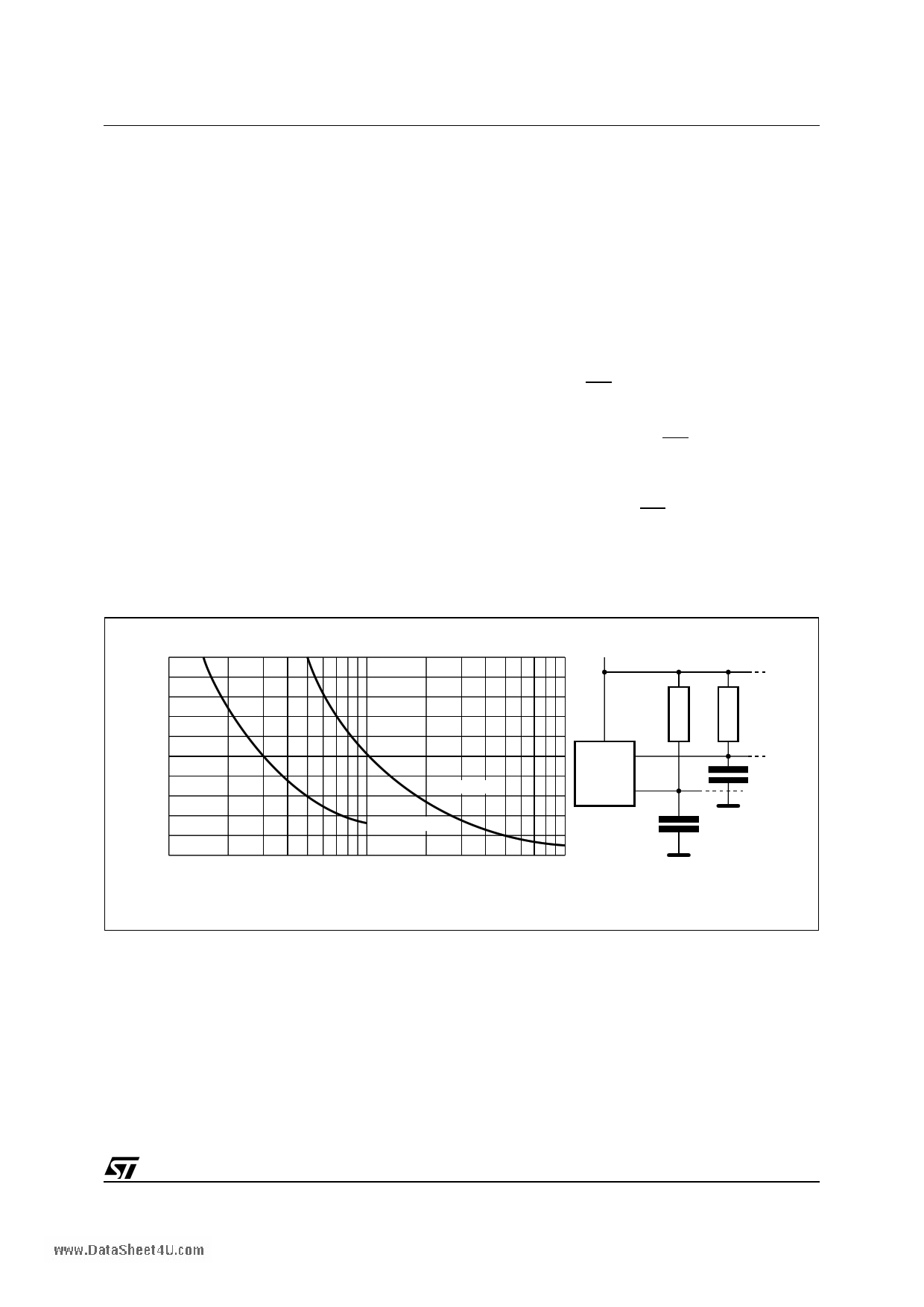
nected from Serial Clock (SCL) to VCC. (Figure 4
indicates how the value of the pull-up resistor can
be calculated). In most applications, though, this
method of synchronization is not employed, and
so the pull-up resistor is not necessary, provided
that the bus master has a push-pull (rather than
open drain) output.
Serial Data (SDA)
This bi-directional signal is used to transfer data in
or out of the device. It is an open drain output that
may be wire-OR’ed with other open drain or open
collector signals on the bus. A pull up resistor must
be connected from Serial Data (SDA) to VCC. (Fig-
ure 4 indicates how the value of the pull-up resistor
can be calculated).
Chip Enable (E0, E1, E2)
These input signals are used to set the value that
is to be looked for on the three least significant bits
(b3, b2, b1) of the 7-bit Device Select Code. In the
end application, E0, E1 and E2 must be directly
(not through a pull-up or pull-down resistor) con-
nected to VCC or VSS to establish the Device Se-
lect Code. When these inputs are not connected,
an internal pull-down circuitry makes (E0,E1,E2) =
(0,0,0).
The E0 input is used to detect the VHV voltage,
when decoding an SWP or CWP instruction.
Write Control (WC)
This input signal is provided for protecting the con-
tents of the whole memory from inadvertent write
operations. Write Control (WC) is used to enable
(when driven Low) or disable (when driven High)
write instructions to the entire memory area or to
the Protection Register.
When Write Control (WC) is tied Low or left
unconnected, the write protection of the first half of
the memory is determined by the status of the
Protection Register.
Figure 4. Maximum RL Value versus Bus Capacitance (CBUS) for an I2C Bus
VCC
20
16
12
8
4
0
10
fc = 100kHz
fc = 400kHz
100
CBUS (pF)
SDA
MASTER
SCL
RL
RL
CBUS
1000
CBUS
AI01665
5/23
5 Page 
Figure 10. Read Mode Sequences
CURRENT
ADDRESS
READ
ACK
NO ACK
DEV SEL
DATA OUT
R/W
www.DataSheet4U.com
M34E02
RANDOM
ADDRESS
READ
ACK
ACK
ACK
NO ACK
DEV SEL *
BYTE ADDR
DEV SEL *
DATA OUT
R/W
R/W
SEQUENTIAL
CURRENT
READ
SEQUENTIAL
RANDOM
READ
ACK
ACK
DEV SEL
DATA OUT 1
R/W
ACK
NO ACK
DATA OUT N
ACK
ACK
ACK
ACK
DEV SEL *
BYTE ADDR
DEV SEL *
DATA OUT 1
R/W
R/W
ACK
NO ACK
DATA OUT N
AI01942
Note: 1. The seven most significant bits of the Device Select Code of a Random Read (in the 1st and 3rd bytes) must be identical.
Read Operations
Read operations are performed independently of
whether hardware or software protection has been
set.
The device has an internal address counter which
is incremented each time a byte is read.
Random Address Read
A dummy Write is first performed to load the ad-
dress into this address counter (as shown in Fig-
ure 10) but without sending a Stop condition.
Then, the bus master sends another Start condi-
tion, and repeats the Device Select Code, with the
RW bit set to 1. The device acknowledges this,
and outputs the contents of the addressed byte.
The bus master must not acknowledge the byte,
and terminates the transfer with a Stop condition.
Current Address Read
For the Current Address Read operation, following
a Start condition, the bus master only sends a De-
vice Select Code with the RW bit set to 1. The de-
vice acknowledges this, and outputs the byte
addressed by the internal address counter. The
counter is then incremented. The bus master ter-
minates the transfer with a Stop condition, as
shown in Figure 10, without acknowledging the
byte.
11/23
11 Page | ||
| Páginas | Total 23 Páginas | |
| PDF Descargar | [ Datasheet M34E02.PDF ] | |
Hoja de datos destacado
| Número de pieza | Descripción | Fabricantes |
| M34E02 | 2 Kbit Serial IC Bus EEPROM Serial Presence Detect | STMicroelectronics |
| M34E04B | 4-Kbit Serial Presence Detect (SPD) EEPROM compatible | STMicroelectronics |
| Número de pieza | Descripción | Fabricantes |
| SLA6805M | High Voltage 3 phase Motor Driver IC. |
Sanken |
| SDC1742 | 12- and 14-Bit Hybrid Synchro / Resolver-to-Digital Converters. |
Analog Devices |
|
DataSheet.es es una pagina web que funciona como un repositorio de manuales o hoja de datos de muchos de los productos más populares, |
| DataSheet.es | 2020 | Privacy Policy | Contacto | Buscar |
