|
|
|
PDF IDT5T9306 Data sheet ( Hoja de datos )
| Número de pieza | IDT5T9306 | |
| Descripción | 2.5V LVDS 1:6 CLOCK BUFFER TERABUFFER II | |
| Fabricantes | Integrated Device Technology | |
| Logotipo | ||
Hay una vista previa y un enlace de descarga de IDT5T9306 (archivo pdf) en la parte inferior de esta página. Total 13 Páginas | ||
|
No Preview Available !
2.5V LVDS 1:6 CLOCK BUFFER
TERABUFFER™ II
www.DataSheet4U.com
IDT5T9306
FEATURES:
• Guaranteed Low Skew < 25ps (max)
• Very low duty cycle distortion < 125ps (max)
• High speed propagation delay < 1.75ns (max)
• Additive phase jitter, RMS 0.159ps (typical) @ 125MHz
• Up to 1GHz operation
• Selectable inputs
• Hot insertable and over-voltage tolerant inputs
• 3.3V / 2.5V LVTTL, HSTL, eHSTL, LVEPECL (2.5V), LVPECL (3.3V),
CML, or LVDS input interface
• Selectable differential inputs to six LVDS outputs
• Power-down mode
• 2.5V VDD
• Available in VFQFPN package
DESCRIPTION:
TheIDT5T93062.5Vdifferential clockbufferisauser-selectabledifferential
inputtosixLVDSoutputs. ThefanoutfromadifferentialinputtosixLVDSoutputs
reduces loading on the preceding driver and provides an efficient clock
distributionnetwork. TheIDT5T9306canactasatranslatorfromadifferential
HSTL, eHSTL, LVEPECL (2.5V), LVPECL (3.3V), CML, or LVDS input to
LVDS outputs. A single-ended 3.3V / 2.5V LVTTL input can also be used to
translate to LVDS outputs. The redundant input capability allows for an
asynchronous change-over from a primary clock source to a secondary clock
source. Selectable reference inputs are controlled by SEL.
The IDT5T9306 outputs can be asynchronously enabled/disabled. When
disabled,theoutputswilldrivetothevalueselectedbytheGLpin. Multiplepower
and grounds reduce noise.
APPLICATIONS:
• Clock distribution
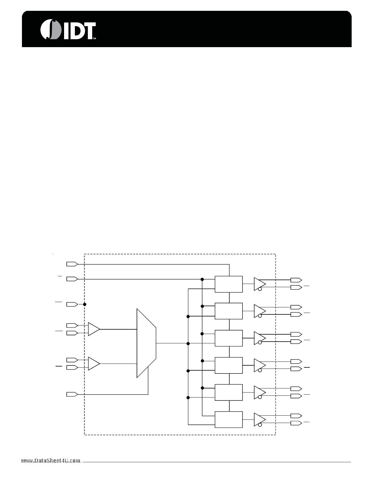
FUNCTIONAL BLOCK DIAGRAM
GL
G
PD
A1 1
A1
A2
0
A2
SEL
OUTPUT
CONTROL
OUTPUT
CONTROL
OUTPUT
CONTROL
OUTPUT
CONTROL
OUTPUT
CONTROL
OUTPUT
CONTROL
Q1
Q1
Q2
Q2
Q3
Q3
Q4
Q4
Q5
Q5
Q6
Q6
IDT™ / ICS™ LVDS CLOCK BUFFER TERABUFFER™ II
1
IDT5T9306 REV. A OCTOBER 23, 2007
1 page 
IDT5T9306
2.5V LVDS 1:6 CLOCK BUFFER TERABUFFER™ II
www.DataSheet4U.com
DIFFERENTIAL INPUT AC TEST CONDITIONS FOR HSTL
Symbol
Parameter
Value
Units
VDIF Input Signal Swing(1)
1V
VX Differential Input Signal Crossing Point(2)
750 mV
DH Duty Cycle
50 %
VTHI InputTimingMeasurementReferenceLevel(3)
Crossing Point
V
tR, tF Input Signal Edge Rate(4)
2 V/ns
NOTES:
1. The 1V peak-to-peak input pulse level is specified to allow consistent, repeatable results in an automatic test equipment (ATE) environment. This device meets the VDIF (AC)
specification under actual use conditions.
2. A 750mV crossing point level is specified to allow consistent, repeatable results in an automatic test equipment (ATE) environment. This device meets the VX specification under
actual use conditions.
3. In all cases, input waveform timing is marked at the differential cross-point of the input signals.
4. The input signal edge rate of 2V/ns or greater is to be maintained in the 20% to 80% range of the input waveform.
DIFFERENTIAL INPUT AC TEST CONDITIONS FOR eHSTL
Symbol
Parameter
Value
Units
VDIF Input Signal Swing(1)
1V
VX Differential Input Signal Crossing Point(2)
900 mV
DH Duty Cycle
50 %
VTHI InputTimingMeasurementReferenceLevel(3)
Crossing Point
V
tR, tF Input Signal Edge Rate(4)
2 V/ns
NOTES:
1. The 1V peak-to-peak input pulse level is specified to allow consistent, repeatable results in an automatic test equipment (ATE) environment. This device meets the VDIF (AC)
specification under actual use conditions.
2. A 900mV crossing point level is specified to allow consistent, repeatable results in an automatic test equipment (ATE) environment. This device meets the VX specification under
actual use conditions.
3. In all cases, input waveform timing is marked at the differential cross-point of the input signals.
4. The input signal edge rate of 2V/ns or greater is to be maintained in the 20% to 80% range of the input waveform.
DIFFERENTIAL INPUT AC TEST CONDITIONS FOR LVEPECL (2.5V) AND
LVPECL (3.3V)
Symbol
Parameter
Value
Units
VDIF Input Signal Swing(1)
732 mV
VX Differential Input Signal Crossing Point(2)
LVEPECL
1082 mV
LVPECL
1880
DH Duty Cycle
50 %
VTHI InputTimingMeasurementReferenceLevel(3)
Crossing Point
V
tR, tF Input Signal Edge Rate(4)
2 V/ns
NOTES:
1. The 732mV peak-to-peak input pulse level is specified to allow consistent, repeatable results in an automatic test equipment (ATE) environment. This device meets the VDIF (AC)
specification under actual use conditions.
2. 1082mV LVEPECL (2.5V) and 1880mV LVPECL (3.3V) crossing point levels are specified to allow consistent, repeatable results in an automatic test equipment (ATE) environment.
This device meets the VX specification under actual use conditions.
3. In all cases, input waveform timing is marked at the differential cross-point of the input signals.
4. The input signal edge rate of 2V/ns or greater is to be maintained in the 20% to 80% range of the input waveform.
IDT™ / ICS™ LVDS CLOCK BUFFER TERABUFFER™ II
5
IDT5T9306 REV. A OCTOBER 23, 2007
5 Page 
IDT5T9306
2.5V LVDS 1:6 CLOCK BUFFER TERABUFFER™ II
Pulse
Generator
VDD
A Qn
A D.U.T.
Qn
RL
VOS
RL
www.DataSheet4U.com
VOD
Test Circuit for DC Outputs and Power Down Tests
Pulse
Generator
VDD/2
A Qn
A D.U.T.
Qn
-VDD/2
CL
Z = 50Ω
Z = 50Ω
CL
SCOPE
50Ω
50Ω
Test Circuit for Propagation, Skew, and Gate Enable/Disable Timing
LVDS OUTPUT TEST CONDITION
Symbol
CL
RL
VDD = 2.5V ± 0.2V
0(1)
8(1,2)
50
Unit
pF
Ω
NOTES:
1. Specifications only apply to "Normal Operations" test condition. The TIA/EIA specification load is for reference only.
2. The scope inputs are assumed to have a 2pF load to ground. TIA/EIA - 644 specifies 5pF between the output pair. With CL = 8pF, this gives the test circuit appropriate 5pF equivalent
load.
IDT™ / ICS™ LVDS CLOCK BUFFER TERABUFFER™ II
11
IDT5T9306 REV. A OCTOBER 23, 2007
11 Page | ||
| Páginas | Total 13 Páginas | |
| PDF Descargar | [ Datasheet IDT5T9306.PDF ] | |
Hoja de datos destacado
| Número de pieza | Descripción | Fabricantes |
| IDT5T9306 | 2.5V LVDS 1:6 CLOCK BUFFER TERABUFFER II | Integrated Device Technology |
| Número de pieza | Descripción | Fabricantes |
| SLA6805M | High Voltage 3 phase Motor Driver IC. |
Sanken |
| SDC1742 | 12- and 14-Bit Hybrid Synchro / Resolver-to-Digital Converters. |
Analog Devices |
|
DataSheet.es es una pagina web que funciona como un repositorio de manuales o hoja de datos de muchos de los productos más populares, |
| DataSheet.es | 2020 | Privacy Policy | Contacto | Buscar |