|
|
|
PDF LC72146M Data sheet ( Hoja de datos )
| Número de pieza | LC72146M | |
| Descripción | PLL Frequency Synthesizer for Electronic Tuning | |
| Fabricantes | Sanyo Semicon Device | |
| Logotipo | ||
Hay una vista previa y un enlace de descarga de LC72146M (archivo pdf) en la parte inferior de esta página. Total 21 Páginas | ||
|
No Preview Available !
Ordering number : EN4922C
CMOS LSI
LC72146, 72146M
PLL Frequency Synthesizer
for Electronic Tuning
Overview
The LC72146 is a PLL frequency synthesizer LSI circuit
for electronic tuning in car stereo systems. The LC72146
supports the construction of high-performance, multi-
functional electronic tuning systems for the VHF MW,
and LW bands.
Features
• High-speed programmable dividers for
— 10 to 160 MHz on FMIN using pulse swallower
— 0.5 to 40.0 MHz on AMIN using pulse swallower
and direct division
• General-purpose counters
— HCTR for 0.4 to 25.0 MHz frequency measurement
— LCTR for 10 to 500 kHz frequency measurement
and 1.0 Hz to 20 × 103 kHz period measurement
• Reference frequencies: Twelve selectable reference
frequencies (4.5 or 7.2 MHz crystal) 1, 3, 5, 9, 10,
3.125, 6.25, 12.5, 25, 30, 50 and 100 kHz
• Phase comparator
— Insensitive band control
— Unlock detection
— Sub-charge pump for high-speed locking
— Deadlock clear circuit
• CCB input/output data interface
• Power-on reset circuit
• Built-in MOS transistor for a low-pass filter
• Inputs/outputs (using five general-purpose input/output
ports)
— Maximum of seven inputs (max)
— Maximum of seven outputs (max/four n-channel
open-drain and three CMOS outputs)
— Time-base output for clock (8 Hz)
• Operating ranges
— Supply voltage ..................................4.5 to 5.5 V
— Opetating temperature ......................–40 to 85°C
• Package
— DIP24S, MFP24S
• CCB is a trademark of SANYO ELECTRIC CO., LTD.
• CCB is SANYO’s original bus format and all the bus
addresses are controlled by SANYO.
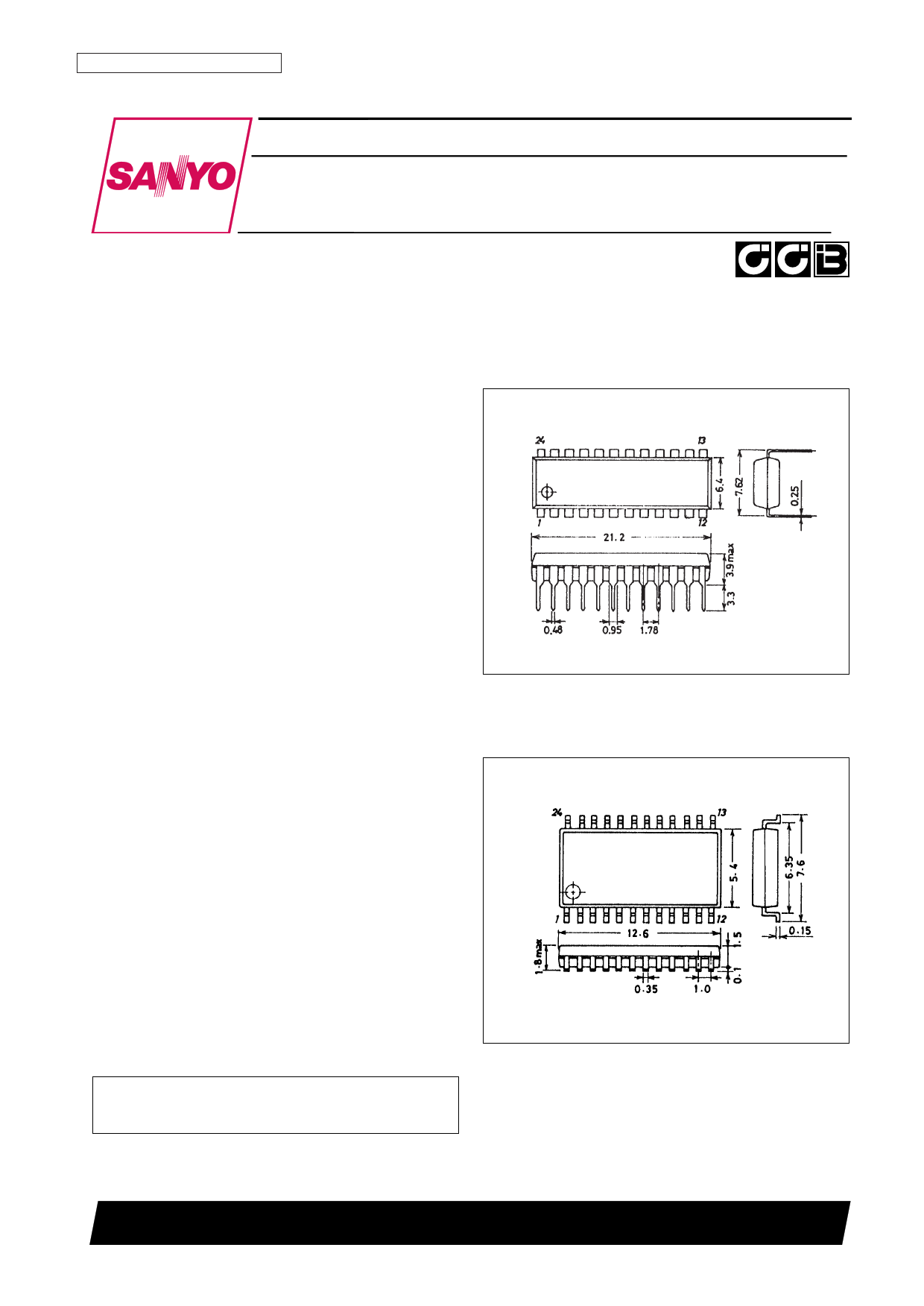
Package Dimensions
unit: mm
3067-DIP24S
[LC72146]
unit: mm
3112-MFP24S
[LC72146M]
SANYO: DIP24S
SANYO: MFP24S
SANYO Electric Co.,Ltd. Semiconductor Bussiness Headquarters
TOKYO OFFICE Tokyo Bldg., 1-10, 1 Chome, Ueno, Taito-ku, TOKYO, 110 JAPAN
73096HA (OT)/11095TH (OT) No. 4922-1/21
1 page 
Pin Functions
Number
Symbol
24 XIN
1 XOUT
LC72146, 72146M
Type
Function
Xtal OSC
Connection for crystal oscillator element (7.2 or 4.5 MHz)
Equivalent circuit
• Serial data input: FMIN is selected when DVS is set to 1.
17
FMIN
Local oscillator Input frequency range: 10 to 160 MHz
signal input • The signal is transmitted directly to the swallow counter
• Divisor value range: 272 to 65535
• Serial data input: AMIN is selected when DVS is set to 0.
• Serial data input: when SNS is set to 1.
• Input frequency range: 2 to 40 MHz
• The signal is transmitted directly to the swallow counter.
16
AMIN
Local oscillator • Divisor value range: 272 to 65535
signal input • Serial data input: when SNS is set to 0.
• Input frequency range: 0.5 to 10 MHz
• The signal is transmitted directly to the 12-bit
programmable divider.
• Divisor value range: 4 to 4095
• IThis pin must be set high to input serial data to the
2
CE
Chip enable
LC72146 DI pin or to output serial data from the DO pin.
• Inputs the clock used for data synchronization when
4
CL
Clock
inputting serial data to the LC72146 DI pin or outputting
serial data from the DO pin.
3
DI
Input data
• Input pin for serial data transmitted to the LC72146 from
a controller.
• Output pin for serial data transmitted from the LC72146 to
5
DO
Output data
a controller.
• The LC72146 power supply connection. A voltage
between 4.5 and 5.5 volts must be supplied when the
15
VDD
Power supply
PLL circuit is used.
• The power on reset circuit operates when power is first
applied.
18
23
VDD
Ground
• The LC72146 ground connection.
12 • General-purpose I/O ports
11
10
I/O-1
I/O-2
I/O-3
• Output mode circuit type: open drain
General-purpose • Function after a power on reset: input port
I/O port
• Can be set up to function as output ports by bits I/O-1 to
I/O-3 in the serial data sent from the controller.
Continued on next page.
No. 4922-5/21
5 Page 
LC72146, 72146M
Continued from preceding page.
No. Name
Function
Related bits
Input/output port control
(7) I/O1 to I/O5 Bits I/O1 to I/O5 set the direction of the ports. Each pin is an input when the corresponding bit is 0,
and an output, when the bit is 1. All ports are set to be inputs after power-on reset.
OUT1 to OUT5, ULD
Output port data
(8)
OUT1 to
OUT7
Bits OUT1 to OUT7 set the output values of the O-1 to O-7 output ports. Each output is open or high when
the corresponding bit is 1, and low, when the bit is 0. A bit is ignored if the corresponding port is an input
port or the unlock output.
I/O1 to I/O5, ULD
Counter input control
Bits H/I-6 and L/I-7 select the operation of the HCTR/I-6 and LCTR/I-7 pins. When H/I-6 is 0, HCTR/I-6 is an
(9) H/I6, L/I7 input port, and when H/I-6 is 1, HCTR/I-6 is the HCTR input. When L/I-7 is 0, LCTR/I-7 is an input port, and
when L/I-7 is 1, LCTR/I-7 is the LCTR input.
CTS0, CTS1
PLL unlock detect control
Bits UL0 and UL1 select the phase error threshold and extension (øE) used to detect the PLL unlocked
state as shown in Table 10 and Figure 4. When the phase error is greater than the selected error, the PLL
unlock detector output goes low.
Table 10 Unlock detection and extension selection
(10) UL0, UL1
UL1
0
0
1
1
UL0
0
1
0
1
Phase error
Stopped
0
±0.56 µs
±1.11 µs
Detector output
Open
øE output
øE with 1 to 2 ms extension
øE with 1 to 2 ms extension
ULD, DT0, DT1
Figure 4 Phase-error extension
Crystal oscillator control
Bit XS selects the oscillator frequency. When XS is 1, the frequency is 7.2 MHz, and when XS is 0,
(11) XS 4.5 MHz.
4.5 MHz is selected after power-on reset.
Phase comparator control
Bits DZ0 and DZ1 select the phase comparator insensitive band, or dead zone.
Table 11 Insensitive band mode selection
(12) DZ0, DZ1
DZ1
0
0
1
1
DZ0
0
1
0
1
Insensitive band (dead zone) mode
DZA
DZB
DZC
DZD
DZA is selected after power-on reset.
Charge pump control
Bit DLC controls the charge pump operation. When DLC is 1, the charge pump outputs are forced to low,
and when DLC is 0, the charge pump operates normally.
(13) DLC This feature can be useful to remove the PLL from a deadlock state. The PLL can deadlock if its VCO
control voltage Vtune becomes 0 V, halting the VCO. Setting DLC to 1 sets Vtune to VCC, restarting the VCO.
Normal operating mode is selected after power-on reset.
An 8 Hz 40% duty clock time base signal can be output from pins 0 to 7 by setting TBC to 1.
(14) TBC When TBC is 1 the OUT7 data will be invalid. TBC is set to 0 by the power-on reset.
Test data
(15)
TEST0 to
TEST2
Bits TEST0 to TEST2 are used for in-factory device testing. Set them all to 0. They are set to zero after a
power-on reset.
OUT7
No. 4922-11/21
11 Page | ||
| Páginas | Total 21 Páginas | |
| PDF Descargar | [ Datasheet LC72146M.PDF ] | |
Hoja de datos destacado
| Número de pieza | Descripción | Fabricantes |
| LC72146 | PLL Frequency Synthesizer for Electronic Tuning | Sanyo Semicon Device |
| LC72146M | PLL Frequency Synthesizer for Electronic Tuning | Sanyo Semicon Device |
| Número de pieza | Descripción | Fabricantes |
| SLA6805M | High Voltage 3 phase Motor Driver IC. |
Sanken |
| SDC1742 | 12- and 14-Bit Hybrid Synchro / Resolver-to-Digital Converters. |
Analog Devices |
|
DataSheet.es es una pagina web que funciona como un repositorio de manuales o hoja de datos de muchos de los productos más populares, |
| DataSheet.es | 2020 | Privacy Policy | Contacto | Buscar |