|
|
PDF TC7WPB9307FC Data sheet ( Hoja de datos )
| Número de pieza | TC7WPB9307FC | |
| Descripción | Low Voltage/Low Power 2-Bit Dual Supply Bus Switch | |
| Fabricantes | Toshiba Semiconductor | |
| Logotipo | ||
Hay una vista previa y un enlace de descarga de TC7WPB9307FC (archivo pdf) en la parte inferior de esta página. Total 13 Páginas | ||
|
No Preview Available !
TC7WPB9306,9307FC/FK
TOSHIBA CMOS Digital Integrated Circuit Silicon Monolithic www.DataSheet4U.com
TC7WPB9306FC,TC7WPB9307FC
TC7WPB9306FK,TC7WPB9307FK
Low Voltage/Low Power 2-Bit Dual Supply Bus Switch
The TC7WPB9306 and TC7WPB9307 are CMOS 2-bit
dual-supply bus switches that can provide an interface between
two nodes at different voltage levels. These devices can be
connected to two independent power supplies. VCCA supports
1.8-V, 2.5-V and 3.3-V power supplies, whereas VCCB supports
2.5-V, 3.3-V and 5.0V power supplies.
Bidirectional level-shifting is possible by simply adding
external pull-up resistors between the An/Bn data lines and the
VCCA / VCCB supplies. There is no restriction on the relative
magnitude of the An and Bn voltages; both the An and Bn data
lines can be pulled up to arbitrary power supplies.
The enable signal can be used to disable the device so that the
buses are effectively isolated.
The Output Enable ( OE :TC7WPB9307, OE:TC7WPB9306)
input is common for all the two-bits of the data lines; thus these
device are used as a single two-bits bus switch. For the
TC7WPB9306, Output Enable (OE) is active-High: When OE is
High, the switch is on; when Low, the switch is off. For the
TC7WPB9307, Output Enable ( OE ) is active-Low: When OE is
Low, the switch is on; when High, the switch is off.
The TC7WPB9306 and TC7WP9307 supports power-down
protection at the OE ,OE input, with OE ,OE being 5.5-V
tolerant.
The channels consist of n-type MOSFETs.
All the inputs provide protection against electrostatic
discharge.
TC7WPB9306FC,TC7WPB9307FC
TC7WPB9306FK,TC7WPB9307FK
Weight
CSON8-P-0.4
SSOP8-P-0.50A
: 0.002 g (typ.)
: 0.01 g (typ.)
Features
• Operating voltage:1.8-V to 2.5-V, 1.8-V to 3.3-V, 1.8-V to 5.0-V, 2.5-V to 3.3-V, 2.5-V to 5.0-V or 3.3-V to 5.0-V
bidirectional interface
• Operating voltage: VCCA = 1.65 to 5.0 V, VCCB = 2.3 to 5.5 V
• Low ON-resistance: RON = 5.0 Ω (typ.)
(ON-resistance test circuit: VIS = 0 V, IIS = 30 mA, VCCA= 3.0 V , VCCB = 4.5 V)
• ESD performance: Machine model ≥ ±200 V
Human body model ≥ ±2000 V
• 5.5-V tolerance and power-down protection at the Output Enable input.
• Packages: CST8,US8
1 2009-03-03
1 page 
TC7WPB9306,9307FC/FK
Electrical Characteristics
www.DataSheet4U.com
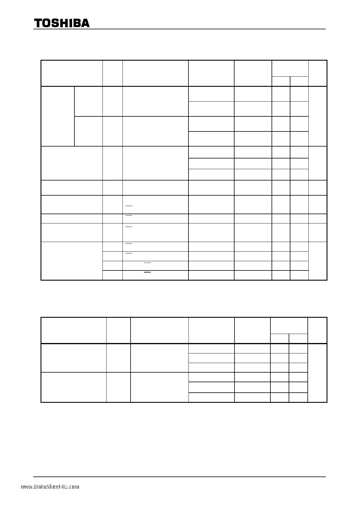
DC Characteristics (Ta = −40 to 85°C)
Characteristics
Symbol
Test Condition
VCCA (V)
High-level
Control input
voltage
VIH
L o w - l e v e l VIL
1.65 ≤ VCCA < 2.3
⎯
2.3 ≤ VCCA < 5.0
1.65 ≤ VCCA < 2.3
⎯
2.3 ≤ VCCA < 5.0
ON-resistance
(Note)
RON
VIS = 0 V, IIS = 30 mA
(Figure 2)
Power off leakage current
Switch-off leakage current
Control input current
leakage current
form VCCB to VCCA
Quiescent supply current
IOFF
An,Bn=0 to 5.5 V
(per circuit)
An,Bn=0 to 5.5 V
ISZ OE = VL ,OE=GND
IIN OE = 0 to 5.5V
ICCBA
OE = 0 or VCCA
VCCB →VCCA
ICCA1
ICCB1
ICCA2
ICCB2
OE = VCCA or GND, IS=0 A
OE = VCCA or GND, IS=0 A
VCCA ≤ OE ≤ 5.5 V, IS=0 A
VCCA ≤ OE ≤ 5.5 V, IS=0 A
1.65
2.3
3.0
0
1.65 to 5.0
1.65 to 5.0
3.3
1.65 to 5.0
1.65 to 5.0
1.65 to 5.0
1.65 to 5.0
VCCB (V)
VCCA to 5.5
VCCA to 5.5
VCCA to 5.5
VCCA to 5.5
2.3
3.0
4.5
0
VCCA to 5.5
VCCA to 5.5
5.0
VCCA
VCCA
VCCA
VCCA
Ta = −40 to
85°C
Min Max
0.8×
VCCA
0.7×
VCCA
⎯
⎯
⎯
⎯
0.2×
VCCA
0.3×
VCCA
⎯ 16.0
Unit
V
⎯ 11.0 Ω
⎯ 8.0
⎯ ±1.0 μA
⎯ ±1.0 μA
⎯ ±1.0 μA
⎯ 10.0 μA
⎯ 1.0
⎯ 1.0
μA
⎯ ±1.0
⎯ ±1.0
Note: ON-resistance is measured by measuring the voltage drop across the switch at the indicated current.
Level Shift Characteristics (Ta = −40 to 85°C)
Characteristics
Symbol
Test Condition
Input/Output Characteristics
(Up Translation)
(Note 1)
VOHU
An = VIN
SW = ON
(Figure 7)
Input/Output Characteristics
(Down Translation)
(Note 2)
VOHD
An = VCCA
SW = ON
(Figure 9)
VCCA (V)
1.65
2.3
3.0
1.65
2.3
3.0
VCCB (V)
3.0 to 5.5
4.5 to 5.5
4.5 to 5.5
3.3 to 5.5
4.5 to 5.5
4.5 to 5.5
Ta = −40 to
85°C
Min Max
1.4 ⎯
2.05 ⎯
2.7 ⎯
1.3 1.65
1.95 2.3
2.6 3.0
Unit
V
Note 1: The Input/Output Characateristics for up translation indicate the input voltages required to provide
VCCA + 0.5 V on the outputs when measured using the test circuitry shown in Figure 7.
Note 2: The Input/Output Characateristics for down translation indicate the voltages that cause the output voltages to
saturate when measured using the test circuitry shown in Figure 9.
5 2009-03-03
5 Page 
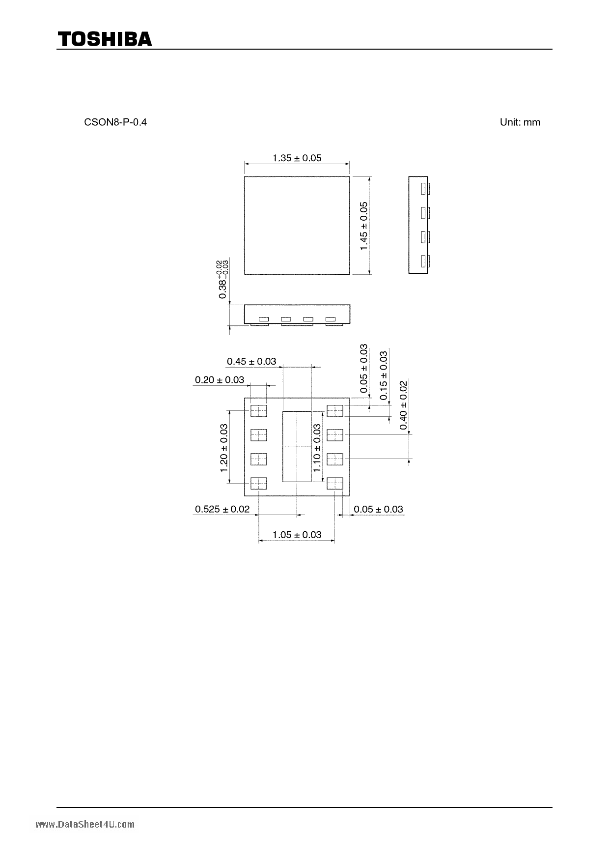
Package Dimensions
TC7WPB9306,9307FC/FK
www.DataSheet4U.com
Weight: 0.002 g (typ.)
11 2009-03-03
11 Page | ||
| Páginas | Total 13 Páginas | |
| PDF Descargar | [ Datasheet TC7WPB9307FC.PDF ] | |
Hoja de datos destacado
| Número de pieza | Descripción | Fabricantes |
| TC7WPB9307FC | Low Voltage/Low Power 2-Bit Dual Supply Bus Switch | Toshiba Semiconductor |
| TC7WPB9307FK | Low Voltage/Low Power 2-Bit Dual Supply Bus Switch | Toshiba Semiconductor |
| Número de pieza | Descripción | Fabricantes |
| SLA6805M | High Voltage 3 phase Motor Driver IC. |
Sanken |
| SDC1742 | 12- and 14-Bit Hybrid Synchro / Resolver-to-Digital Converters. |
Analog Devices |
|
DataSheet.es es una pagina web que funciona como un repositorio de manuales o hoja de datos de muchos de los productos más populares, |
| DataSheet.es | 2020 | Privacy Policy | Contacto | Buscar |
